


 English
TURN-KEY PCB ASSEMBLY: BITTELE ELECTRONICS
PCB MANUFACTURING AND ASSEMBLY
Full Turn-Key PCB Manufacturer
You can quickly get quotes and order PCB fabrication and assembly using our online system. Take advantage of exclusive automatic discounts with our tool. Our BOM pricing tool ensures you receive the lowest price for your order.
START A TURN-KEY PCB ORDER
A Brief Analysis of the Most Common Surface Mount Devices (SMDs)
Bittele Electronics is an experienced provider of Complete PCB Assembly for all package types, with over 10 years of industry experience in providing High-Quality PCB Assembly for Surface Mount Devices (SMDs) of all sorts. In this article, we would like to offer our clients some insight into six common types of SMDs, including the standard applications of these package types, as well as their effects on the PCB Assembly Process. In the interest of brevity, we will not delve into too much detail here with regard to the specifics of PCB design around these parts. For a complete picture of our processes where these parts are concerned, please see our individual articles on PLCC, QFP, QFN, BGA, and POP components, as well as our comprehensive DFA Guidelines document.
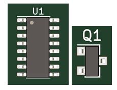
SOIC & SOT
The SOIC (Small Outline Integrated Circuit) and the SOT (Small Outline Transistor) are perhaps the most common type of SMDs, and are included in a majority of SMT Assembly projects today. The SOIC can be considered the surface-mount equivalent of the classic though-hole DIP (Dual-Inline Package), while the SOT is a direct SMD equivalent to the legacy through-hole SOT package.
Both of these package types are included under Bittele’s PCB Options at a Standard Price, and no additional cost or PCB Turn Time will be incurred by the presence of these types of components on your Bill of Materials (BOM). This means that our standard PCB Assembly Process is sufficient to effectively assemble SOIC and SOT components with no additional tooling or process engineering required.
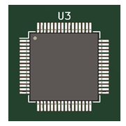
QFP
QFP (Quad Flat Package) components are most often used for microcontrollers, multi-channel codecs, and other moderately complex parts. They are generally considered the simplest option for high pin-count components, since the leads of a QFP are exposed and therefore relatively easy to inspect rework if necessary.
QFPs are also included in Bittele’s PCB Options at a Standard Price, and are treated just the same as any other SMD for the purposes of quotation and assembly. As with all SMDs, the number of pads included on the package will have some impact on the price of your quotation, but no additional cost is added for the simple existence of a QFP component in your design. These parts can be assembled using standard Reflow Soldering, and inspected using Automated Optical Inspection (AOI) in tandem with multi-stage Visual Inspection.
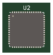
QFN
The QFN (Quad Flat No-Lead) package is similar to the QFP, with the notable difference that the electrical contacts of these devices do not protrude from the body of the component. This difference allows for QFN packages to be physically smaller than equivalent QFPs, but they do require some additional attention during PCB Assembly, and generally cannot be assembled reliably by non-professional methods such as Manual Assembly.
Unlike the package types discussed above, QFN packages do require some additional attention during PCB Assembly. The most notable difference in process for these parts is that they require X-Ray Inspection as a part of the Quality Management process. For designs with only a few small QFN packages, we can sometimes waive additional costs associated with these more demanding inspection procedures, but this must be assessed on a case-by-case basis.
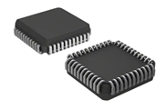
PLCC
PLCCs (Plastic Leaded Chip Carriers) are flexible options that allow for components to be mounted in a socket or soldered directly onto the PCB. These packages are particularly convenient for Prototype PCB Assembly projects, and especially those requiring IC Programming services. A socket can be used in the early iterations of the PCB, allowing ICs to be easily swapped in and out for testing purposes, and the smaller footprint of the IC itself can even be placed within the larger socket footprint so that no design change is necessary when your project moves into larger scale production.
PLCC sockets are normally treated as QFP-type components for the purposes of PCB assembly, while the PLCC components themselves are more akin to QFNs. As such, you should expect a slight difference in your PCB Assembly Quote when you switch to the more permanent solution of soldering your PLCC chip directly to the board. That being said, this cost is offset by the often considerable cost of IC sockets that will no longer need to be included on your BOM at this stage.
BGA
BGA (Ball Grid Array) packages are generally used for the most complex, high pin-count components on the market today, such as high-speed microprocessors and FPGAs (Field Programmable Gate Arrays). That being said, smaller BGA Variants such as the µBGA and DSBGA are sometimes used for simpler components for their smaller size compared to other package types. All BGA variants will require Reflow Soldering for their PCB Assembly, since the electrical contacts of these parts are located entirely beneath the silicon body of the IC.
Similar to QFN packages, BGAs will require additional attention from Bittele’s process engineers in the form of X-Ray Inspection. Since these parts are so complex and sensitive, and include such a multitude of pins that must all be soldered perfectly, we do require X-Ray inspection for BGA Assembly projects to ensure that we can meet our guaranteed standards of quality.
POP
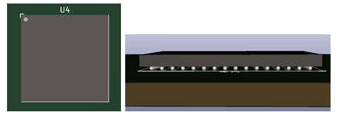
POP (Part-on-Part) technology refers to a process whereby specific components can be assembled directly atop one another. Most commonly used for memory modules and their associated microprocessors, this technique allows for significant space conservation in High-Density Interconnect (HDI) designs, as well as high-speed communication between crucial devices. The bottom device is normally a large BGA component with a high pin count, and a ring of additional BGA-style contacts on the top of the device, as shown in the image below.
POP Assembly is quite complex, and requires special attention during the PCB Assembly Process. Notably, the presence of these parts on a BOM will often require multiple placement and/or Reflow Soldering cycles, which does require additional cost and lead time compared to other component types. Bittele strongly recommends that clients whose designs include POP components reach out to our PCB Customer Service team early in the design process, and send along any preliminary PCB Design Files you might have available. Early collaboration will allow our production team to prepare a strategy for your POP design ahead of time, and also to make DFM (Design for Manufacturing) or DFA (Design for Assembly) suggestions to reduce the cost and lead time associated with these complex parts.
There are of course many other types of SMDs on the market, but our aim in this article is to cover the basics for our clients. The information included here can often be extrapolated to gain some idea of Bittele’s process requirements for all sorts of surface mount parts. For any questions regarding specific packages not included here, or for a more detailed look at these component types, we highly recommend the additional resources mentioned in the introductory paragraph above. You can also Contact Us any time to send along your questions, or to get an official quotation for your project today.
Sequential Lamination: The Backbone of PCB Fabrication
The most fundamental manufacturing technique in modern PCB Fabrication is Sequential Lamination. Simply put, this term describes the process of building up a PCB layer by layer, using multiple subcomposites of copper and insulating PCB Laminate Material. This technique allows for the completion of complex tasks such as trace routing on internal copper layers, as well as the drilling of Blind and Buried Vias. Without Sequential Lamination, it simply would not be possible to produce the complex High-Density Interconnect (HDI) PCBs that are steadily becoming more commonplace across all electronics industries. So how does this important technology work, and what do you need to know as a PCB designer to ensure a flawless Sequential Lamination process for your upcoming project with Bittele?

The good news here is that your responsibilities regarding Sequential Lamination are fairly straightforward. Among your PCB Design Files should be a document called the PCB Multi-Layer Stackup, which describes the order and specific thicknesses of each layer to be laminated together. Bittele’s production engineers can even provide assistance in creating a detailed stackup for your project, including complex considerations such as Impedance Control. If your HDI design does require special attention for features such as Micro-Vias, we recommend that you refer to our comprehensive DFM Guidelines document for complete details on our capabilities and design rules where these elements are concerned.
With your stackup completed, you can leave the actual specifics of the Sequential Lamination process to us. Bittele’s process engineering team will build your PCB from the middle out, starting with the Prepreg and working out to the external surfaces of the finished board. The copper layers are subjected individually to trace routing, and blind/buried vias are drilled out as each new layer is laminated onto the board in progress. The actual lamination process involves state of the art PCB Fabrication machinery that is able to apply high amounts of temperature and pressure to the subcomposites, adhering them permanently to one another. Once the lamination is complete, any mounting holes and through vias are drilled through the fully laminated product, and your order is all set for the final stages of Silkscreen, Surface Finish, and finally the PCB Assembly Process can begin.
We hope that this brief explanation has acted to clear up any queries or uncertainties you might have had with regard to the Sequential Lamination process. If you do have any remaining questions, we would be happy to hear from you! To send along those questions, or to get an official quotation for our Complete PCB Assembly services today, you can Contact us over email at sales@7pcb.com, or give us a call toll-free at 1-888-812-1949.
PTFE Teflon PCBs
PTFE (Polytetrafluoroethylene) is the scientific name for a very well-known product, even outside the engineering community; DuPont’s trademarked Teflon has applications extending far beyond your kitchen, and into many high-speed electronic devices across a variety of industries. At Bittele Electronics, we are proud to offer a wide variety of PCB Laminate Materials for our clients’ convenience, including multiple varieties of PTFE laminates from Rogers. This article is intended to provide Bittele’s clients with basic information regarding these High-Frequency PCB Materials, as well as their effects on the PCB Assembly Process, in order to facilitate a more informed decision making process where PCB materials are concerned.
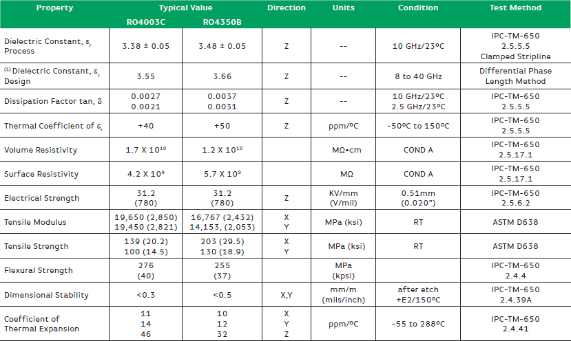
As mentioned briefly above, PTFE materials are valued for their suitability in high-frequency applications. At RF and Microwave frequencies, the dielectric constant of standard FR-4 Material (approx. 4.5) is often too high, resulting in significant signal loss during transmission across the PCB. Fortunately, PTFE materials boast dielectric constant values as low as 3.5 or below, making them ideal for overcoming the high-speed limitations of FR-4. The most common of these PTFE PCB materials were developed by Rogers, and are denoted by an “RO” prefix in their product name. In addition to a reduction in dielectric constant, these materials also offer very impressive thermal characteristics for High Temperature PCB applications, reaching Tg values as high as 280°C. A datasheet comparison is shown below for two different PTFE materials, RO4003C and RO4350B.
Of course, every product has its benefits and its drawbacks, and PTFE material is no exception to this rule. Perhaps most importantly, PTFE material, unlike FR-4, is not included among Bittele’s PCB Options at a Standard Price, and the cost of this material is significantly greater than standard FR-4.
PTFE materials also require additional care during PCB Fabrication due to a few specific aspects of the material itself, relative to standard FR-4. First of all, PTFE materials are rather soft, making them prone to gouging or tearing while PCB Routing and PCB Drilling operations are performed. The other main concern during production relates to PTFE’s most well-known aspect: this material is used to coat frying pans and cookpots because of the slick, non-stick surface it provides. Unfortunately, this same property can make it difficult to produce Plated Through-Holes and Slots, since the copper plating requires specialized techniques to seed the PTFE with metal for bonding. These complications also contribute to the higher cost of PCB Fabrication for PTFE materials.
Since PTFE is only necessary for specialized applications, we do not always carry stock for all different types of common PTFE laminates. Be sure to check in with our PCB Customer Service Experts well in advance of your order to ensure that we can provide the material you require.
PTFE is an incredibly useful material for PCB Fabrication and PCB Assembly, but its advantages must be weighed carefully against its costs in order to maximize the economy of your PCB project. If you need any help in these assessments, Bittele Electronics is happy to be of assistance in any way we can. You can Contact Us for advice any time at sales@7pcb.com, or toll-free at 1-888-812-1949.