


 English
TURN-KEY PCB ASSEMBLY: BITTELE ELECTRONICS
PCB MANUFACTURING AND ASSEMBLY
Full Turn-Key PCB Manufacturer
You can quickly get quotes and order PCB fabrication and assembly using our online system. Take advantage of exclusive automatic discounts with our tool. Our BOM pricing tool ensures you receive the lowest price for your order.
START A TURN-KEY PCB ORDER
Micro-VIA on HDI PCBs
What are the differences between VIA and micro-via and why are they used? What are the benefit and costs of using micro-via with HDI circuit boards? How do you design micro-via in HDI PCBs and what are the differences of different design structures?
What are VIA?
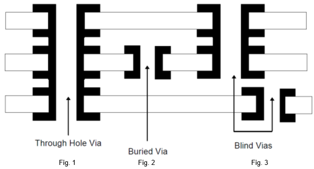
Notably VIA is a feature in PCB fabrication meaning Vertical Interconnect Access forming electrical connections from one copper layer to another in a PCB. A via consists of three main parts: the barrel which is the conductive tubing linking two layers passing through a hole in the PCB formed by drilling or laser, the pad connected to the ends of the barrel connecting the barrel to components, planes or traces, finally the anti-pad or the clearance hole separating the barrel and the copper layers. VIA are separated into three types the through-via, blind-via, and buried via.
In fact, when people think of via what they think of is usually a through-via. This is the conventional plated-through-hole (PTH) via where holes are drilled through from one side of the board to the other side and plated. It has access to both of the external layers of the PCB board like shown in Fig. 1.
When designing a High-Density Multi-layered Printed Circuit Board (PCB) we use the various types of micro-via such as blind via and buried via . These types of micro-via are used in High density interconnect (HDI) technology to make more complex PCBs. Micro-via consists of tiny holes with a diameter of 6 mils or less in circuit boards made by using laser. These holes are plated to connect adjacent layers allowing a PCB to hold more circuit traces which increases the board’s circuit density. A standard micro-via only links two adjacent copper layer and so there are more space available for holding trace lines.
Regarding buried-via that are hidden inside the board they are invisible from the outside since they only pass between the inner layers. While buried-via can pass through two or more inner layers buried-via cannot pass through to any outer layer thus the drilling must be done during the assembly process of the PCB not at the end. Buried via only connects the internal layers like shown in Fig. 2 without access to the external layers.
Furthermore, there are blind-via which can only be seen on one side of the board. It connects an outer layer and can pass through two or more layers connecting to any inner layers. However blind-via cannot pass through the entire board connecting directly to the other outer layer and like shown in Fig. 3 it must connect to one of the external layers.
What are Micro-Via used for?
Considering the fact that fast advancements in new techniques like micro-via and HDI technology are always due to market demands we can conclude that the technology is in demand. Currently the trend in the electronics industry is constantly towards designing smaller, lighter and higher functionality electronic devices. To make a device smaller and lighter means the PCB must also be smaller and lighter. To increase functionality means the PCB routing must become more complex. A need for smaller PCBs was created as newer and smaller components such as the Ball Grid Arrays (BGAs) came onto the market due to the higher numbers of I/Os. I/Os are basically input and outputs connected to component so when the number of I/Os increase this means an increase in the number of circuits traces necessary in the same board area.
Various solutions have been suggested to adapt to the miniaturization of new components in electronic assemblies. One solution is the use of High Density Interconnect (HDI) technology with micro-via to connect the various copper layers. By using various via the PCB can hold more circuit traces meaning a denser placement of components. The aim is to increase circuit density using mainly micro-via and blind-via with a few buried-via and the regular through-via to reduce the area of the PCB. Micro-via and HDI technology make it possible to hold six components in the same space where originally four components in a conventional fan out routing could be held meaning micro-via can reduce the area necessary for circuit boards.
Why use Micro-Via?
In fact, using standard micro-via is preferred in HDI PCB board design due to their reliability. The performance of HDI boards using micro-via is much better compared to conventional PCBs due to their trace routes’ shorter length and diameter. Shorter distance for signals to travel means reduction of internal noise improving signal quality and strength. Conventional circuit boards also have some tiny capacitive loads and stubs in the wiring resulting in signal degradation. However, micro-via can reduce any parasitic loads due to shorter wiring distances and eliminate stubs. In addition, by filling and capping the micro-via it is also possible to reduce inductance in the HDI board.
Costs
Generally using new HDI and micro-via technology always costs more compared with when using older techniques. Considering the key factors of the new technique’s cost increase was the increase in the number of steps by about 8 to 10 for the manufacturing process and the cost for materials used in the conductive fill of the via. Micro-via mainly has non conductive epoxy, conductive epoxy, copper filled, silver filled and electrochemical plating to fill the via. The more via traces there are in a design the more via fills needed so the cost for these via fills can be calculated as proportional to the number of via and their sizes in the design.
On balance designers can compensate for this increase in cost due to the process and new materials by using HDI and micro-via more actively. HDI technology can use space in a circuit board more efficiently resulting in a higher wire routing density. This allows the board size to be smaller since a smaller area can hold more connections in the board. Also the vertical connections made using the micro-via allows the large routing channels to be put on other layers. By using these vertical connections, we can reduce the size and the number of layers in a board to offset the cost of using the new micro-via technology. For example, when using a HDI board with micro-via technology it is possible to reduce an 8-layer PCB into a 4-layer HDI PCB.
HDI design
Obviously for a HDI PCB board the circuit routes need to interconnect several layers to connect components. However, it is best to use micro-via when possible in a board since it is the most reliable type of interconnection structures. But standard micro-via can only be used to connect two adjacent layers in a High-Density Multi-layered Printed Circuit Board (PCB). Thus in order to achieve the best result possible we use micro-via with complex structures.
Hence in order for the circuit routes to connect more than two adjacent layers we use micro-via in compound design structures. Complex structures which uses standard micro-via are of two types which are staggered and stacked structures. Of these two types the staggered design structures are used by placing micro-via with small offsets between layers. This is the most reliable complex design structure but it requires slightly more space in the HDI PCB design.
The second complex design type is stacking the micro-via on top of each other. This way uses space more efficiently achieving the highest possible circuit density and is easier to use than staggering structure. Unfortunately, your stacking micro-via would make them less reliable due to the via experiencing greater thermal stress during the solder reflow step thus they are considered to be less reliable then through-via. Buried-via inside the board can also be used with stacking structures but they are the least reliable since they depend on their formation.
Conclusion
In essence when choosing to design an HDI board it should be a planned use of HDI technology not just used as a last resort because a designer failed to route the circuit on a conventional board. Careful planning and knowledge of the procedures involved in building the board is necessary to take full advantages of HDI and micro-via technology. Thus it is better at the beginning of a complex design project to assess the benefits and costs involved with choosing to use HDI technology. Due to it being a new process if you design the board the same way as with conventional boards would only add costs with no benefits. Thus in order to reduce the cost of using the new micro-via technology we must use the advantages granted by this technology to reduce the area of the circuit board increasing the savings shipping due to the board being smaller. Also consulting technicians familiar with the materials and construction process allowing designer to reduce the numbers of layers in a HDI board using less material and steps thus reducing costs.
Related Articles:
Please briefly describe the information you are seeking in the search bar below.