


 English
TURN-KEY PCB ASSEMBLY: BITTELE ELECTRONICS
PCB MANUFACTURING AND ASSEMBLY
Full Turn-Key PCB Manufacturer
You can quickly get quotes and order PCB fabrication and assembly using our online system. Take advantage of exclusive automatic discounts with our tool. Our BOM pricing tool ensures you receive the lowest price for your order.
START A TURN-KEY PCB ORDER
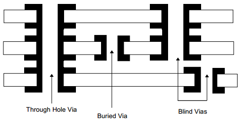
Blind and Buried Via PCBs
Blind and/or buried vias are similar to traditional, multi-layer PCBs with through-holes in that these via create connections between layers of the PCB. But one important difference is that blind and buried vias do not necessarily connect all layers of a board. This difference permits circuits of non-planar topography to be connected, which traditional multi-layer boards can’t do. This is an important advantage since it economizes the use of space on the board by permitting only the required layer be connected.
Bittele Electronics applies specific definitions to the various types of drilled interconnections. They are:
- Through-hole via: on that can be accessed from both external layers of the board
- Blind via: one that doesn’t go through the complete board yet can be accessed by one of the external layers of the board.
- Buried via: one that only makes connections with the inner layers of the board and is not accessible by any of the external layers
Stacked Micro-via
Stacked micro-via is a type of compound design structure which stacks micro-via on top of each other. Stacked micro-via use space efficiently allowing you to achieve the highest possible circuit density and are easier to use than a staggered structure. Unfortunately, stacked micro-via are less reliable as the via experiences greater thermal stress during the solder reflow step. Consequently, they are considered to be less reliable even less compared to a though-via.
Staggered Micro-via
Staggered micro-via is a type of compound design made by placing micro-via with small offsets from each other between layers. This is the most reliable complex design structure but it requires slightly more space in the HDI PCB design.
Difference between Buried and Blind Vias:
Blind Vias are such vias which connect an outer layer to one or multiple inner layers thus they have an opening on the outer layer whereas buried vias are the ones which are buried between the outer layers and they only interconnect the inner layers.
Purpose of Buried and Blind Vias:
Space on the PCB board can be saved using buried and blind vias which allow the PCB tracks to be run over or under them without getting shorted. Most fine pitched BGA and flip chip IC footprints don’t support tracks to run under them or have vias. Here we can use buried or blind vias that avoid making connection to unwanted layers in a particular region thus saving precious space on the PCB.
Cost of Buried and Blind Vias:
Since blind and buried vias must be drilled through only some layers, they must be drilled and plated before the board layers are completely combined. Thus, multiple lamination steps are required compared to one lamination for through holes. These extra steps add time and cost to your order. However, the benefits of this technology outweigh the extra cost in many cases.
See Design Limitations of Blind and Buried Vias for more information on PCB designs using these vias.
Related Articles:
Please briefly describe the information you are seeking in the search bar below.