


 English
TURN-KEY PCB ASSEMBLY: BITTELE ELECTRONICS
PCB MANUFACTURING AND ASSEMBLY
Full Turn-Key PCB Manufacturer
You can quickly get quotes and order PCB fabrication and assembly using our online system. Take advantage of exclusive automatic discounts with our tool. Our BOM pricing tool ensures you receive the lowest price for your order.
START A TURN-KEY PCB ORDER
Splitting Interconnect Blind Vias Into Stack-up Vias
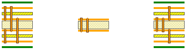
Manufacturing PCBs with interconnect blind vias seems harder than it is. For instance, on a 4-layer PCB, a stack up with vias from layer 1 to 2, layer 2 to 3, and layer 3 to 4 is ok, but a stack up with vias from layer 1 to 2, layer 1 to 3, layer 4 to 3, and layer 4 to 2 seems too difficult. In reality there is no difference. The solution is to split the vias and stack them. So split the 1 to 3 drill into 1-2 & 2-3. Same with 4-2 drill, split it into 4-3 & 3-2. This way you stack them up as 1-2 over 2-3, and 4-3 over 3-2 drill.
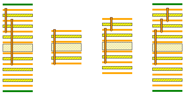
When stacking vias you must fill the ones in the inner layers for the laser to reflect back from the smooth surface. Failure to do so will result in dimples at the via hole locations and may result in voids. There are various options available for filling vias. Vias can be filled with resin, NCVF (non-conductive via fill) and copper fill. Copper filling is the most common for microvias as it is the best thermal conductor among all of the above options, however it is expensive. Resin fill is the most economical of them all.
Following pictures show how to split interconnect vias into stack-up vias, making the manufacturing process much more simplistic.
A lamination cycle is pressing PCB layers together with plating on the outside. When splitting interconnect vias into stacked vias, you would be adding more lamination cycles. Although this increases the price a bit due to the extra process steps involved, it is the best option to manufacture such boards.
For example, if there is an 8 layer stack up with vias from layer 1 to 3 and from layer 2 to 6, the easiest solution is to split it up into vias from layer 1 to 2, layer 2 to 3, and layer 3 to 6, and do it in 3 lamination cycles. First, press layers 3 to 6 together and drill the vias through them. Next, press layers 2 and 7 onto the board and drill the vias from layer 2 to 3. Finally, press the top and bottom layers onto the board and drill the vias from layer 1 to 2. In this situation it is usually preferable to do a foil build, however a core build will work equally well.
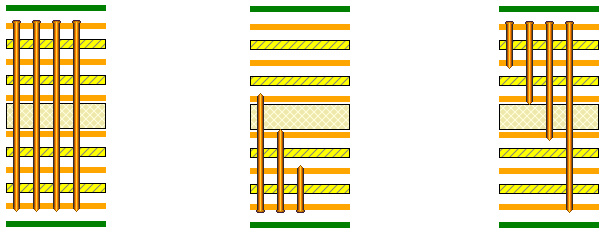
Back-drilling is the process of drilling all of the layers straight through then using control depth drilling from the other side to sever all unnecessary connections. For example, if there is a 6 layer stack up with vias from layer 1 to 2, layer 1 to 3, layer 1 to 4, and a normal drill straight through the board, the easiest solution is to drill all of the holes straight through and then back-drill from layer 6 to 3, layer 6 to 4, and layer 6 to 5, thereby severing all unwanted connections. This a cost effective solution because control depth drilling is more economical than multiple lamination cycles with laser drilled microvias. However, this option is only possible when the PCB does not have too many tight pitched BGAs or tight spacing. Also, the PCB layout has to accommodate the technology, making sure no traces are running at the back drill locations or they will be cut.
In the case of microvias, the drill size must be greater than the thickness of the dielectric. Generally, PCB manufacturers like to keep dielectrics at least 1 MIL smaller than the laser drill hole. It is possible to have multiple drill sizes in the same laser drill file so long as the smallest of them is greater than the thickness of the dielectric.
Mechanical drill size depends on aspect ratio, which is the ratio of the board thickness to the drill size. This table shows minimum mechanical drill sizes for some standard board thickness and their aspect ratios:
| THICKNESS | MINIMUM DRILL SIZE | ASPECT RATIO |
|---|---|---|
| 0.031” | 0.010” | 3.1:1 |
| 0.042” | 0.010” | 4.2:1 |
| 0.062” | 0.010” | 6.2:1 |
| 0.093” | 0.017” | 5.47:1 |
| 0.125” | 0.019” | 6.58:1 |
Related Articles:
Please briefly describe the information you are seeking in the search bar below.