


 English
TURN-KEY PCB ASSEMBLY: BITTELE ELECTRONICS
PCB MANUFACTURING AND ASSEMBLY
Full Turn-Key PCB Manufacturer
You can quickly get quotes and order PCB fabrication and assembly using our online system. Take advantage of exclusive automatic discounts with our tool. Our BOM pricing tool ensures you receive the lowest price for your order.
START A TURN-KEY PCB ORDER
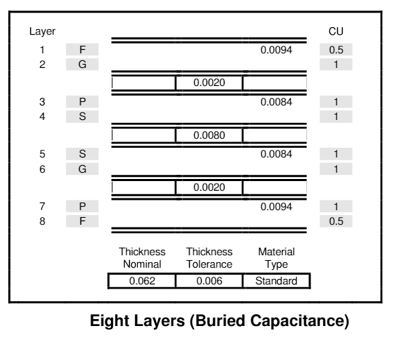
Buried Capacitance
How Decoupled Capacitance can be Obtained without Components?
The goal of designing PCBs is to make them for the least amount of money while designing the best ways for them to perform well. Most people would say you cannot have both goals. However, new technological developments are helping engineers realize this goal by improving the high frequency electromagnetic interference performance while keeping costs down.
This technology is called Buried Capacitance. It is both patented and licensed across the world. It uses ZBC-2000 laminate material. In brief, it is a PCB producing methodology that spreads decoupled capacitance by inserting them in tiny dielectric layers inside the PCB and next to the power areas. This methodology essentially eliminates the need for decoupling capacitors. What this does is free up more space on the PCB and it helps designers make PCBS that have greater performance, or the same performance in a smaller board size.
Desired Buried Capacitance Examples
The diagrams inserted below give the popular ways that Buried Capacitance can be used. If you need more information, you can
Contact Us
by email at
sales@7pcb.com.
Related Articles:
Please briefly describe the information you are seeking in the search bar below.