


 English
TURN-KEY PCB ASSEMBLY: BITTELE ELECTRONICS
PCB MANUFACTURING AND ASSEMBLY
Full Turn-Key PCB Manufacturer
You can quickly get quotes and order PCB fabrication and assembly using our online system. Take advantage of exclusive automatic discounts with our tool. Our BOM pricing tool ensures you receive the lowest price for your order.
START A TURN-KEY PCB ORDER
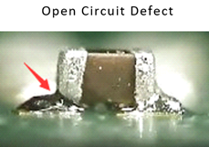
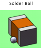
Tombstoning and Solder Balls
It is possible to have too much of a good thing. The Solder Mask on your PCBs protects against the formation of Solder Bridging during PCB Assembly, and it provides additional high-voltage insulation between traces and copper planes. High quality solder mask is one of the clearest and most vital advantages of professional PCB Fabrication. Maintaining a sufficient solder mask thickness is crucial to the integrity of your finished boards, but too much solder mask can lead to PCB Tombstones, open circuit defects, or the formation of solder balls.

How can too much Solder Mask thickness cause faults?
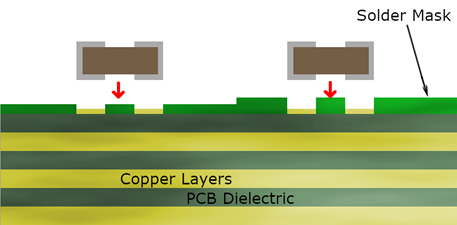
Inappropriate solder mask thickness can cause issues like tombstones and solder balls as easily as commonly known culprits, such as uneven sizing of SMT pads, or capillary action from Via in Pad. In fact, the reason that these issues can come from a thick solder mask is perhaps the easiest to understand. As shown in the diagram below, a very thick solder mask can prevent smaller components like passives from sitting fully atop their SMT pads during Reflow Soldering. As a result, the part may lean further toward one pad, causing a tombstone or open circuit defect. Solder paste is also more likely to escape from the pad and form solder balls when the component is not mounted securely.
How Can Bittele Help?
At Bittele Electronics, we have carefully tailored our PCB Assembly Process over years of experience in the industry. We can confidently guarantee a solder mask of minimum 5 µm thickness near conductor corners, and 10 µm thickness on conductor surfaces. In order to protect your boards from assembly defects, we also ensure that the solder mask thickness does not extend too high beyond these minimum values. The maximum for solder mask thickness depends upon the Copper Weight, so get in touch with us if you need to specify a thickness for your project. For standard 1 oz. copper, we normally control for 40 µm solder mask thickness at the most.
The good news about this is that clients of Bittele will almost never have to worry about specifying appropriate solder mask thickness, since we follow a standard process to ensure appropriate levels. If you find yourself in the uncommon scenario where you need to specify a particular solder mask thickness for your project, make sure to get in touch with us early in the design process so we can work with you. Our engineering team will be happy to help with Design for Manufacturing (DFM) and Design for Assembly (DFA) on your boards to get you the best possible outcome on your PCBs.
If find yourself with any other questions about the solder mask on your PCBs, you can reach out to us any time! Our PCB Customer Service specialists are ready to help you understand our capabilities, tolerances, and processes so you can get the best possible result for your PCB project.
Related Articles:
- PCB Solder Mask, Mask Options, Colours & Impact of Mask Colour
- How Important Are Solder Masks and Silkscreens
- Bittele’s Solder Mask Webbing Capabilities
- How to Prevent the Tombstone and Open Defects during the SMT Reflow Process
- Which Soldering Defects are Related to the Incorrect Setup of the Reflow Profile?
Please briefly describe the information you are seeking in the search bar below.