


 English
TURN-KEY PCB ASSEMBLY: BITTELE ELECTRONICS
PCB MANUFACTURING AND ASSEMBLY
Full Turn-Key PCB Manufacturer
You can quickly get quotes and order PCB fabrication and assembly using our online system. Take advantage of exclusive automatic discounts with our tool. Our BOM pricing tool ensures you receive the lowest price for your order.
START A TURN-KEY PCB ORDER
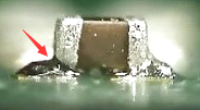
How to Prevent the Tombstone and Open Defects during the Reflow Process
The tombstone phenomenon is a defect that occurs when passive SMT components are partially or completely lifted from the PCB pad. What usually occurs is that one end of chip is soldered on the PCB pad while opposite end of the chip stand ups vertically, looking similar to a tombstone in a cemetery.
Analysis of Root Causes
The root cause of the tombstone phenomenon is that the wetting properties (e.g., different wetting speeds) cause an imbalanced torque at the two ends of the chip terminals when the solder paste starts to melt. The tombstone phenomenon has other causes, including:
-
The solder pads are improperly designed:
- The components’ terminals are not covered by more than 50% of PCB pads due to the space between the two pads is too wide.
- The two pads are designed with different sizes.
- The solder paste printing is uneven.
- The component placement is inaccurate.
- The reflow oven temperature is uneven.
- The thermal conductivity of the PCB material has different heating capacities.
- The presence of nitrogen has a tendency to increase the occurrence of the tombstone defect.
- Placing the chip parallel with the reflow oven’s conveyor.
Corrective Actions
- Design the pad sizes according to the recommendation specified on the datasheet.
- Reflow profile -- for lead-free solder paste, use a gradual soak ramp rate before reaching the melting point.
- Improve the accuracy of the solder paste printing.
- Impove the accuracy of chip placement by decreasing the placement speed.
- Esnure the pick and place nozzles have been adjusted to the correct pressure.
Another phenomenon is the OPEN circuit defect. This occurs when there is an electrical continuity OPEN circuit between at least one terminal of the chip and the solder pad. This phenomenon is very critical because even AOI cannot detect this failure most of the time.
Analysis of Root Causes
The root cause of the OPEN circuit phenomenon is similar to the tombstone defect. However additional causes must be considered:
- Component oxidization has occurred.
- The pad sizes are not correct. The component’s terminals are not covered by more than 50% of PCB pads due to the space between the two pads is too wide.
- There is poor flux activity.
Corrective Action
- Design the pad sizes according to the recommendation specified on the datasheet.
- Select new components.
- Reflow profile -- for lead-free solder paste, use a gradual soak ramp rate before reaching the melting point.
- Adjust the pressure for pick and place nozzles.
Related Articles:
- Which Soldering Defects are Related to the Incorrect Setup of the Reflow Profile?
- How to Prevent Solder Ball and Bridging Defects during the SMT Reflow Process
- How to Prevent Non-Wetting Defect during the SMT Reflow Process
- How to Prevent Solder Bridging in 3528 PLCC6 RGB LEDs?
- An Analysis of SMT Solder Paste Printing Defects
Please briefly describe the information you are seeking in the search bar below.