


 English
TURN-KEY PCB ASSEMBLY: BITTELE ELECTRONICS
PCB MANUFACTURING AND ASSEMBLY
Full Turn-Key PCB Manufacturer
You can quickly get quotes and order PCB fabrication and assembly using our online system. Take advantage of exclusive automatic discounts with our tool. Our BOM pricing tool ensures you receive the lowest price for your order.
START A TURN-KEY PCB ORDER
How to Prevent Solder Ball and Bridging Defects
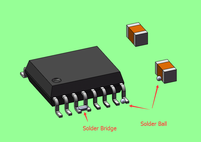
A solder ball is the most common type of defect that occurs in the SMT assembly process. Solder balls located within 0.13mm of traces violate the minimum electrical clearance principle. They can adversely affect the electrical reliability of the assembled PCB.
According to the IPC A 610 standard, a PCB is also considered defective when there are 5 solder balls (<=0.13mm) within 600mm^2.
Analysis of Root Causes
The solder ball is very closely related to air or water (trapped in solder paste) vapour escaping from the paste and turning into liquid. If the vapor in solder paste escapes too fast, a small amount of liquid solder will be taken from from soldering joint, and a solder ball will be formed when it cools down.
-
PCB contains water.
- Stored in an unexpectedly humid environment and isn’t dried before assembly.
- PCB is too new and was not dried enough.
- Too much flux is applied in the solder paste.
- The preheat temperature is not high enough, so the flux has failed to effectively vapour out;
- A solder paste printing issue due to the stencil not being clean, which causes the solder paste to stick to unexpected areas.
Corrective Actions
- Design the correct pad sizes and spaces according to the recommendation specified in the datasheet.
- Reflow profile – when appropriate increase the preheating temperature.
- Bake the PCB before printing.
- PCB quality -- The thickness of PCB hole’s plating copper is greater than 25μm in order to avoid trapping water in the PCB.
Solder Bridging is another common defect, which occurs when the solder has formed an abnormal connection between two or more adjacent traces, pads or pins, and forms a conductive path.
Analysis of Root Causes
- There is no solder mask between adjacent pads.
- The pads are spaced too close to one another.
- There are residues stuck on the PCB surface or pads.
- A dirty stencil with paste sticking on its underside.
- A misalignment during solder paste printing.
- A misalignment when components are placed on the board.
- Excessive placement pressure will squeeze the paste out of the pads.
- Paste slump has occurred or too much paste is applied to the pads.
- The preheat temperature is not high enough, so the flux has not activated.
Corrective Action
- Add solder mask between the pads.
- Design the pads and stencil aperture to the right size.
- Do not mix old and new flux together.
- Adjust the solder paste printing pressure.
- Adjust the pressure for pick and place nozzles.
- Ensure there is a zero print gap between the PCB and the stencil.
- Clean the stencil as quickly as possible.
Related Articles:
- Which Soldering Defects are Related to the Incorrect Setup of the Reflow Profile?
- How to Prevent the Tombstone and Open Defects during the SMT Reflow Process
- How to Prevent Non-Wetting Defect during the SMT Reflow Process
- How to Prevent Solder Bridging in 3528 PLCC6 RGB LEDs?
- An Analysis of SMT Solder Paste Printing Defects
Please briefly describe the information you are seeking in the search bar below.