


 English
TURN-KEY PCB ASSEMBLY: BITTELE ELECTRONICS
PCB MANUFACTURING AND ASSEMBLY
Full Turn-Key PCB Manufacturer
You can quickly get quotes and order PCB fabrication and assembly using our online system. Take advantage of exclusive automatic discounts with our tool. Our BOM pricing tool ensures you receive the lowest price for your order.
START A TURN-KEY PCB ORDER
Understanding Solder Ball Formation in SMT Process
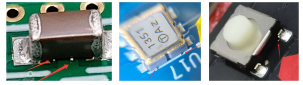
Solder balls are one of the most common defects in SMT (Surface Mount Technology) production. They typically appear on the sides between the terminals of chip components, and occasionally around IC packages or inside the leads of tactile switches (as shown in the figures). These solder balls usually range from 0.2 mm to 0.3 mm in diameter.
How Are Solder Balls Formed?
During the reflow soldering process, solder paste and flux begin to activate as the reflow oven temperature gradually rises. The solder paste transitions from a paste to a viscous semi-liquid and eventually melts into a fully liquid state. During this phase, flux vaporize and release gases forming air bubbles.
These bubbles, under the influenced by surface tension and thermal expansion may either escape, expand, or combine with other bubbles. The pressure caused by flux vapor expansion can produce tiny solder spheres (metal particles) and separate from the solderpaste. These may move outside the pad area and settle on the solder mask edge. Upon cooling, these free solder particles solidify as solder balls.
Why Are Solder Balls a Problem?
Solder balls not only affect the appearance of electronic products but more importantly, it also causes functional risk. During product use, these solder balls will detach and cause short circuits between adjacent pins or components, ultimately compromising final product reliability and electrical performance.
Therefore, effective control and prevention of solder balls through process optimization is essential for improving overall SMT soldering quality and product stability.
Root Causes of Solder Ball Formation
1. Solder Paste Surface Tension and Wetting Behavior
- A. Solder Paste Flowability: When the solder paste reaches its melting point (typically around 217 °C or higher), it liquefies. Due to surface tension, if the tension is too high, the solder may not spread evenly across the pad, causing local buildup. Upon cooling, this solder can solidify into solder balls.
- B. Solder Paste Breakdown: During the preheat stage, the flux component of the paste begins to evaporate. If the paste’s surface tension is too low, it may go out and overflow beyond the pad area, which can lead to solder ball formation around the pad.
2. Flux Activity and Composition
- A. Function of Flux: Flux is responsible for removing oxides and contaminants from the metal surfaces of the PCB and components. It also prevents reoxidation during the soldering process, ensuring proper wetting and joint formation.
- B. Inadequate Flux Activity or Improper Composition: If the flux is not sufficiently active or improperly formulated, it may fail to remove oxides effectively. This results in poor wetting between the solder and the metal surfaces, increasing the likelihood of solder ball formation.
3. Airflow Effects
- A. Reflow Oven Airflow: Improper airflow settings or PCB layout can cause turbulent air currents in certain zones of the reflow oven. These currents may disturb molten solder, displacing it and leading to solder ball formation.
- B. Temperature Gradient-Induced Airflow: Varying temperatures between different reflow zones can generate air currents, affecting solder paste flow and wetting behavior.
4. PCB Pad Design Factors
- A. Pad Geometry and Spacing: Oversized or undersized pads, irregular pad shapes, or insufficient spacing between components can lead to uneven solder paste distribution, increasing the risk of solder ball formation.
- B. Pad Surface Finish: Poor surface finish or surface contamination can inhibit proper solder wetting during reflow, causing solder to move outside the pad area and form solder balls.
5. Component Lead Design
- A. Component Lead Shape: Leads that are too long, too short, uneven, or oxidized can prevent proper wetting between the lead and the pad, resulting in solder balls.
- B. Pad-to-Lead Compatibility: If the component lead size does not match the pad design, solder paste may be squeezed out during placement, forming solder balls after reflow.
- C. Lead Pitch: Tight lead spacing may cause solder to move to adjacent pad and make solder bridging, contribute to form solder balls.
6. Reflow Profile Settings
- A. Improper Preheat Ramp-Up: If the temperature rises too quickly in the preheat zone, moisture and flux solvents in the solder paste may not fully evaporate before reaching peak temperature. This can cause boiling and solder splatter in the reflow zone, forming solder balls.
- B. Optimized Thermal Profile: A well-designed reflow profile should match the solder paste and component specifications, allowing full paste reflow, even wetting, and high-quality joint formation.
7. PCB Handling and Storage
- A. PCB Surface Contamination and Oxidation: Surface treatments such as ENIG, HASL, or OSP may diminish if improperly handled or stored, contaminants and oxidation on the PCB surface reduce solderability and increase solder ball defects.
- B. Moisture and Cleanliness Control: Maintain good PCB surface integrity by preventing moisture absorption, dust, and oil contamination during storage or handling.
- C. Silkscreen Misalignment: If the silkscreen overlapped the pad surface or misaligned, it could obstruct solder paste flow outside the stencil window, causing paste to buildup outside the pad area and form solder balls.
8. Placement Height and Pressure
- A. Misaligned Placement Height: Improper placement height may shift or tilt components, causing to uneven solder paste distribution and buildup, leading to solder balls.
- B. Excessive Placement Pressure: Over-pressure during placement can force solder paste to spread beyond the pad area, forming balls after reflow.
- C. Height Optimization by Component Type: Placement height should be adjusted based on component body height to avoid squeezing the solder paste excessively.
9. Solder Paste Ǫuality and Usage Control
- A. Solder Paste Composition and Consistency: Low-quality solder paste may contain impurities, inconsistent viscosity, or poor metal-to- flux ratios, which all lead to uneven melting, incomplete reflow and solder ball formation.
- B. Usage Handling: Solder paste must be stored, mixed, and used according to manufacturer guidelines to prevent degradation or contamination.
- C. Environmental Control: High humidity in the production area can cause solder paste to absorb moisture, reducing shelf life and increasing the risk of solder balls.
- D. Workshop Standards: Maintain a clean, temperature and humidity-controlled production environment to ensure stable solder paste behavior.
10. Stencil Aperture Design Issues
- A. Misalignment and Oversized Aperture: Poor stencil alignment or oversized apertures can cause solder paste to overflow and fail to reflow back onto the pad, forming solder balls.
- B. Lack of Anti-Solder Ball Design Features: If the stencil lacks in anti-solder ball design strategies (e.g., reduced outer edge apertures or chamfered cuts), paste may escape from pad boundaries more easily, increasing defect rates.
Preventive Measures to Reduce Solder Ball Formation
1. PCB Pad Design and Component Selection
During PCB layout, select appropriate component packages and ensure recommended supplier pad dimensions and spacing are properly matched to the component leads or terminals for optimal solderability and minimize spread out of excess solder paste.
2. Incoming PCB Material Inspection
Ensure incoming PCBs are properly packaged, within shelf-life limits, and free from surface contamination or oxidation. Pads should be clean, and silkscreen should not overlap or exceed pad boundaries. Boards with poor packaging should be baked or stored in a dry cabinet before use.
3. Strict Solder Paste Management
Maintain the activity and printability of solder paste by following proper storage, handling, and usage protocols. Monitor paste condition and avoid contamination or degradation.
4. Optimized Reflow Profile Settings
Adjust the preheat temperature ramp-up rate based on the specific characteristics of the solder paste and components to ensure complete flux evaporation before reflow.
5. Stencil Aperture Optimization
Adjust stencil aperture size and shape based on component dimensions and pad layout to ensure proper solder volume and minimize paste overflow.
6. Root Cause Analysis of Solder Ball Defects
When solder balls are found during production, conduct root cause analysis promptly and implement corrective actions to prevent recurrence.
Understanding the physical and chemical behavior of solder paste and flux during reflow is key to minimizing solder ball defects. By optimizing process parameters such as stencil design, paste selection, reflow profile, and flux formulation manufacturers can significantly reduce solder ball occurrence and enhance the reliability and performance of SMT assemblies.
For more information about our capabilities or to send us your PCB Design Files for an official quotation, please feel free to Contact Us any time! We can be reached via email at sales@7pcb.com or call at 1-416-800-7540.
Related Articles:
Please briefly describe the information you are seeking in the search bar below.