


 English
TURN-KEY PCB ASSEMBLY: BITTELE ELECTRONICS
PCB MANUFACTURING AND ASSEMBLY
Full Turn-Key PCB Manufacturer
You can quickly get quotes and order PCB fabrication and assembly using our online system. Take advantage of exclusive automatic discounts with our tool. Our BOM pricing tool ensures you receive the lowest price for your order.
START A TURN-KEY PCB ORDER
LGA Package Module Soldering Process
1. Background
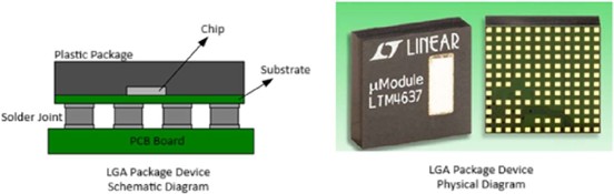
a. Land Grid Array (LGA) Package
The Land Grid Array (LGA) is a type of area array package that is structurally similar to a Ball Grid Array (BGA). It has gained widespread adoption due to its compact footprint, low mounting profile, and high reliability. Unlike BGA packages, which feature solder balls on the bottom, LGA components have only flat metallic pads (lands) or terminals at the bottom of the package without any solder balls.
b. SMT Soldering Challenges for LGA Modules
- PCB Warpage During Reflow: The LGA module and the PCB board can experience warpage during reflow soldering due to thermal expansion and contraction. This issue becomes more pronounced as the size of the LGA module increases.
- Tight Solder Mask Clearance: The small gap between the solder mask of the module and to the pads of PCB limits flux volatilization during reflow. This often results in solder joint defects such as voids and air entrapment.
- Insufficient Solder Volume on Pads: The copper pads in PCB board have limited solder capacity can lead to solder paste may overflow during placement, resulting to solder balls or bridging defects.
- Post-Soldering Inspection Difficulty: Visual inspection is not feasible for LGA solder joints. Inspection must rely on X-ray analysis or functional testing.
- Inspection Limitations: Post-soldering inspection is challenging due to the lack of visual access. X-ray inspection or functional testing is required to verify solder joint integrity.
Our company frequently assembles such components. However, after implementing improvements to reduce solder balls, we encountered a high defect rate due to insufficient solder and cold joints. Analysis showed that when stencil aperture area was approximately 80% of the PCB pad with 0.12 mm stencil thickness, cold joints were eliminated but solder balls persisted. Conversely, reducing the aperture area to 50% eliminated solder balls but resulted in over 80% cold joint failure rate. In mass production, a trade-off had to be made between solder balling and cold joints, prioritizing solder joint reliability and manually removing solder balls post-reflow as needed.
2. Improvement Plan
a. Preliminary Evaluation
Collaborate with the customer to confirm that they can provide test fixtures for in- process verification of module soldering quality. This allows for process parameter experimentation without risking large-scale quality issues, enabling data-driven optimization.
b. Stencil Design Optimization
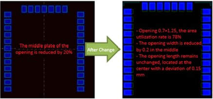
- Pad Sizing Review: Based on component datasheet and actual pad measurement, the PCB land pads are designed in a 1:1 ratio with the LGA module pads, aligning with component datasheet recommendations and design standards.
- Edge Clearance Consideration: A 0.14 mm gap exists between the module pads and the module edge. This may be intentional to prevent damage to the pad during module fabrication. However, during reflow, solder paste may not retract fully, leading to solder balls on the outer edge. Therefore, outer stencil apertures should be reduced.
- Pad Spacing Constraints: The spacing between adjacent PCB pads is only 0.2 mm. A full-size aperture (1:1 width) could cause solder bridging due to paste overflow during placement. Aperture width should be reduced, and spacing increased to mitigate this risk.
- Warping Compensation: Due to varying degrees of module warpage, historical data suggests that maintaining stencil aperture area at approximately 80% of the pad area is necessary to ensure optimal soldering results with reliable solder joints.
- Electro-polishing Finish on Stencil: Use electro-polishing on the stencil after laser cutting to reduce aperture wall roughness. This enhance solder paste printing by minimizing paste adhesion to the aperture walls.
- Gerber Files Verification: Request the panelized Gerber files from the customer to ensure that stencil apertures align precisely with PCB pad layout.
c. Solder Paste Printing
- Solder Paste Viscosity Check: When use freshly opened solder paste for the initial print. Scoop the stirred solder paste with the squeegee to a height of 75–100 mm above the container. Let it fall vertically. Acceptable solder paste should initially flow like thick syrup and break into segments as it falls. If paste does not fall, it is too thick; if it flows continuously without breaking, it is too runny and has low viscosity. Confirm that the solder paste viscosity is within acceptable limits.
- Print Ǫuality Inspection: After setting the printing parameters, inspect the solder paste deposits under a magnifier to ensure full and well-formed, with no signs of breaking. Use a solder paste thickness tester to verify that the thickness variation is within the acceptable range. Once parameters are finalized, it saves and keep unchanged during mass production.
d. Component Placement
Inspect the placement results visually. From a side view, the solder paste should remain intact without overflow or deformation, and the component should appear to “float” on the paste. Ensure the component is aligned within the silkscreen outline on the PCB, with no misalignment or positional deviation. Once placement parameters are confirmed, it remains untouched for mass production.
e. Reflow Soldering
Control the temperature ramp-up rate in the preheat zone to 2–3 °C/s. Maintain the soak zone at 150–190 °C for approximately 90 seconds. The time above 217 °C should be around 60 seconds for reflow zone, with a peak temperature of 240–245 °C. Once the thermal profile is verified to meet specifications, lock the parameters for production.
f. Inspection and Testing
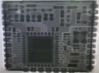
After reflow, perform visual inspection to ensure there are no visible solder balls. With x-ray inspection of 80 units revealed no solder bridging or cold joints will be set standards. Customer feedback must confirm they no issues in electrical and functional testing. However, solder voids remain an area for ongoing improvement.
3. Summary
a. Comprehensive Process Optimization
Achieving high-quality soldering for LGA components requires a holistic process approach. This improvement initiative focused on optimizing the soldering process for LGA pad-type modules by refining stencil aperture design, printing, placement, and reflow parameters. The results is validated through X-ray inspection and customer testing which demonstrated a significant reduction in solder balls while maintaining solder joint integrity. Among all improvements, stencil aperture optimization and placement parameter accuracy were the most critical factors.
b. Areas for Continued Improvement
Solder voids and air entrapment remain visible after reflow. Industry consensus attributes void formation primarily to two factors:
- Flux Volatilization: Solder paste contains flux, which includes 40–60 wt% volatile solvents.
- Moisture Outgassing: Moisture can be trapped in PCB resin or microcracks during fabrication. During reflow, this moisture vaporizes and escapes, forming voids. This is why pre-baking PCBs is essential. Additionally, both PCBs and solder paste can absorb ambient moisture if exposed to air for extended periods, contributing further to void formation.
For applications with strict voiding requirements, pre-tinning the module may be used as a mitigation strategy. In production, using highly active solder paste can also significantly reduce bottom-side voids.
For more information about our capabilities or to send us your PCB Design Files for an official quotation, please feel free to Contact Us any time! We can be reached via email at sales@7pcb.com or call at 1-416-800-7540.
Related Articles:
Please briefly describe the information you are seeking in the search bar below.