


 English
TURN-KEY PCB ASSEMBLY: BITTELE ELECTRONICS
PCB MANUFACTURING AND ASSEMBLY
Full Turn-Key PCB Manufacturer
You can quickly get quotes and order PCB fabrication and assembly using our online system. Take advantage of exclusive automatic discounts with our tool. Our BOM pricing tool ensures you receive the lowest price for your order.
START A TURN-KEY PCB ORDER
How to Prevent Solder Bridging in 3528 PLCC6 RGB LEDs?
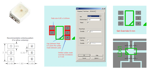
The 3528 PLCC RGB LED*, such as theLG LEMCS32F00AZ01, has ultra high brightness in a compact size. Heat dissipation should be considered during layout design. The traces that connect each LED pad should be designed as wide as possible. Pad sizes need to follow the manufacturer’s recommended land pattern. However, we still found there was very big amount of the solder bridging defect (0.1%) occurring in the prototype stage.
Solder bridging occurs randomly between LED pads. It is pretty hard to detect because it could be happening underneath the components. Only a functional test can tell you what’s wrong with the light color emitting LED.
When we checked the LED pads on a bare PCB with a microscope, we observed there there was no solder mask in the gap between the pads. Furthermore, after we reviewed the pads’ design in EDA software and found that the size of the pad’s solder mask override was 0.106mm (4 mil) as the default value. But the gap between the pads was only 0.2mm as per the manufacturer’s recommendation. It was less than twice the solder mask override (2 x 0.106 = 0.212mm). This confirmed that there was no solder mask between the pads. When we placed the LED onto the board, the solder paste on the pads was squeezed to the edge of the pads. It was possible for them to be in contact with one another because the gap was small. We think this was root cause of the defect.
The next step was to redesign the pads’ solder mask size. We set up manually the solder mask override value to 0.
We also redesigned a new stencil for paste printing with a shrinking aperture size width from 0.65mm to 0.55mm and an extending aperture size length from 0.85 to 0.95 mm.
The production results were very positive. The solder bridging defects dropped down to zero in the following 10,000 pcs assembly.
* 3528 (body size 3.5 x 2.8 mm) PLCC (6-pin package) RGB LED
Related Articles:
- Which Soldering Defects are Related to the Incorrect Setup of the Reflow Profile?
- How to Prevent Solder Ball and Bridging Defects during the SMT Reflow Process
- How to Prevent the Tombstone and Open Defects during the SMT Reflow Process
- How to Prevent Solder Joint Voiding and Cold Solder Defects during the SMT Reflow Process
- How to Indicate Placement Orientation of Diodes and LEDs on Your PCBs
Please briefly describe the information you are seeking in the search bar below.