


 English
TURN-KEY PCB ASSEMBLY: BITTELE ELECTRONICS
PCB MANUFACTURING AND ASSEMBLY
Full Turn-Key PCB Manufacturer
You can quickly get quotes and order PCB fabrication and assembly using our online system. Take advantage of exclusive automatic discounts with our tool. Our BOM pricing tool ensures you receive the lowest price for your order.
START A TURN-KEY PCB ORDER
How to Prevent Short Circuits to Ground in QFNs?
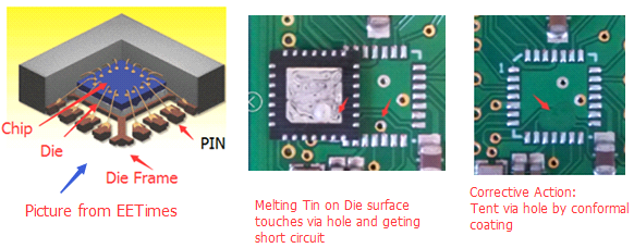
The QFN-type package is getting popular because of its small form factor. It also can be easily reeled without any lead damage compared to other packages such as QFP, SOP and TSSOP. Since these devices are typically less than 14 mm on one side, the exposed die is designed under the center of the chip in order to dissipate heat efficiently. This exposed die, made of copper and usually with a tin finish, is connected to the chip’s ground pin in most situations.
In the PCB layout design stage, the designer should consider adding the same size exposed copper pan in the center of QFN land pattern. This offers a heat conduit for thermal relief that makes the components work with more stability.
In some situations, when the component does not consume a lot of power in order to get hot, the exposed copper on the PCB also can be removed, especially in high density applications. But pay close attention: if there are via holes under the IC, they must be tented by solder mask because during reflow, the finishing tin on the IC dies will melt when the temperature reaches 217°C (lead-free SAC305 solder paste) so there is more risk of touching the exposed via hole and causing an unexpected short circuit. Especially, if the PCB is new without any pad oxidization, it is very easy to cause a short circuit.
Furthermore, the designer also needs to avoid placing other components such as chip resistors and capacitors close to the corner of ICs (See picture, 8 points at 4 corners) because there are die frames exposed to the edge of the IC, mostly 2 point’ at one corner. Other chip terminals have a big chance of makinv contact at those exposed points if they are too close to each other. If they are too close, they will cause another type of short circuit defect as well.
Related Articles:
- How to Prevent Solder Bridging in 3528 PLCC6 RGB LEDs?
- How to Prevent Solder Ball and Bridging Defects during the SMT Reflow Process
- How to Prevent the Tombstone and Open Defects during the SMT Reflow Process
- How to Prevent Solder Joint Voiding and Cold Solder Defects during the SMT Reflow Process
- An Analysis of SMT Solder Paste Printing Defects
Please briefly describe the information you are seeking in the search bar below.