


 English
TURN-KEY PCB ASSEMBLY: BITTELE ELECTRONICS
PCB MANUFACTURING AND ASSEMBLY
Full Turn-Key PCB Manufacturer
You can quickly get quotes and order PCB fabrication and assembly using our online system. Take advantage of exclusive automatic discounts with our tool. Our BOM pricing tool ensures you receive the lowest price for your order.
START A TURN-KEY PCB ORDER
Common QFN Issues and How to Avoid Them
At Bittele Electronics, we are fully dedicated to providing straightforward, efficient, low-cost, and customer-focused High Quality PCB Assembly. One of our main goals along this theme is to recognize and rectify any potential faults that could occur at any point in the PCB Assembly Process. When QFN packages are present on a board, we take extra care to ensure the integrity of the project, since QFN Reworking can be rather difficult.
As a PCB designer, your main responsibility is simply to ensure that the footprint in your CAD design matches the land pattern indicated on the QFN part’s datasheet, and that all spacing and tolerance requirements fall within Bittele’s guidelines. For a detailed view of our PCB Fabrication and PCB Assembly capabilities, please see our DFM Guidelines and DFA Guidelines documents.
This article will proceed with a brief overview of the specific areas that have some potential to cause a fault, as identified through more than a decade of industry experience. These are the most common issues that we notice at Bittele through our pre-fabrication DFM Checking process and our post-assembly X-Ray Inspection methods. Clients who choose our Complete PCB Assembly service for their QFN components should familiarize themselves with these common issues, and design around them whenever possible.
Via in Pad
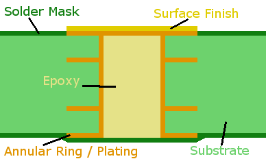
If your PCB design specifies vias within SMT pads, we call the associated production process “Via in Pad” or “Active Pad”. In these cases, there is a risk of solder leakage through the pads during assembly, resulting in a corrupted solder joint that must be reworked after the Reflow Soldering process. In order to combat this difficulty, a non-conductive epoxy is generally used to fill the via hole, while the walls remain plated for electrical conductivity. If the vias are small enough and few enough, it may be possible to just fill the holes with solder mask with no risk to your boards.
Solder Bridging
A short may occur during assembly if there is an insufficient amount of Solder Mask between pins. Designing boards without properly distributing the weight of the components can also contribute to this issue, so be sure to check on the physical aspects of your parts as well as their electrical attributes. It is very important to design the pads making sure to leave enough space between them and the solder mask layer. Component alignment issues may also occur if a proper X-Y (Centroid) File is not implemented, as it is very important to the SMT assembly. For a detailed example on how to generate pick and place files on Eagle, Altium and ORCAD/ALLEGRO, see our complete instructions on how to create a Centroid File from Eagle, Altium and ORCAD/ALLEGRO? .
Clearances
Proper PCB Component Spacing is of the utmost importance when dealing with QFN packages. Part-to-part spacing is not usually an issue in our experience, but in an effort to meet increasingly stringent HDI requirements, it is not infrequent for us to receive designs that violate our part-to-hole or part-to-board-edge requirements. If copper traces are pulled too close to the edge of the board, damage is likely to occur when the individual PCBs are routed from the larger Panelized PCB.
Plating voids
Insufficient copper plating on the inside walls of holes on the PCB. The can cause the boards to be defective as the electrical current will not be able to pass between the layers. We can avoid this by ensuring that the holes are thoroughly and properly cleaned after drilling. This helps to prevent any contamination of the material or air bubbles inside of it.
De-Wetting / Non-Wetting
De-wetting can occur when the molten solder does cover a lead or pad, but then retreats and leaves behind a mound of solder. Non-wetting occurs when the solder only partially covers a surface, leaving some exposed copper behind. Both of these issues can be avoided by making sure the component parts are still within their usable shelf lives and the flux being used must not be past it’s prime (after long hours of use).
If you have any further questions about our QFN Assembly capabilities, or to get started on your project with Bittele today, you can Contact Us over email at sales@7pcb.com, or toll-free at 1-888-812-1949. Bittele Electronics is a Canadian PCB Assembly service provider, based out of Toronto, but serving clients worldwide since 2003.
Related Articles:
Please briefly describe the information you are seeking in the search bar below.