


 English
TURN-KEY PCB ASSEMBLY: BITTELE ELECTRONICS
PCB MANUFACTURING AND ASSEMBLY
Full Turn-Key PCB Manufacturer
You can quickly get quotes and order PCB fabrication and assembly using our online system. Take advantage of exclusive automatic discounts with our tool. Our BOM pricing tool ensures you receive the lowest price for your order.
START A TURN-KEY PCB ORDER
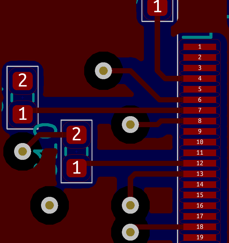
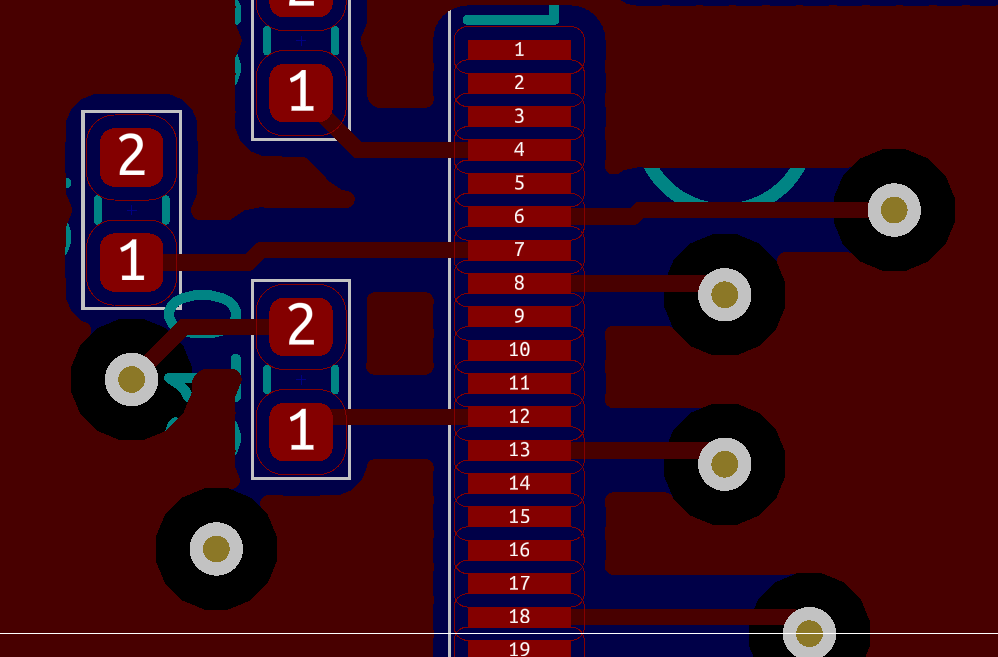
Part-to-Part, Part-to-Hole Spacing
The spacing and land pattern design for each component package will impact the overall reliability and timeline requirements for the PCB Assembly Process, and will also have a considerable impact on the repairability of a PCB. In order to help our customers make the most out of their Turnkey PCB experience, Bittele Electronics has established clear guidelines for controlling component spacing for maximum efficiency during production. Along with our minimum requirements, you’ll find here some general advice on the topic of component spacing for your PCB Design.
Part-to-Part Spacing
Adequate spacing between components on the board protects against potential faults such as solder bridging, and allows for easier manual soldering and/or rework. The greater the part-to-part spacing, the better in terms of quality and ease for PCB Assembly, but Bittele does understand that certain applications will require tight spacing to achieve an altogether small form factor.
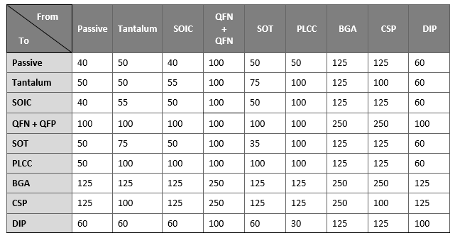
The table provided below shows Bittele’s minimum spacing requirements between various surface mount parts. Measurements in this table are given in mil (thousandths of inches). Measurements should be either from the edge of the pad or the part body, whichever is the smaller distance.
A few special cases should also be noted on the topic of part-to-part spacing for sensitive packages, such as BGA, POP, or larger QFP/QFN:
- IC sockets should be spaced as far as possible from sensitive packages. Frequent loading and unloading of the IC into the socket will place undue stress on nearby solder joints
- Sensitive packages should not be placed in the center of a PCB, since this is where the maximum bow & twist tends to occur, which can result in broken connections
- BGA and other lead-less packages should be placed only on one side of the PCB. If they must be placed on both sides, they should not be in the same x-y positions (“on top of” each other), since this will greatly complicate X-Ray inspection and rework.
Part-to-Edge Spacing
Part-to-edge spacing refers to the distance from a given component a PCB to the board edge. This condition is important for the depanelization process, which is performed after PCB assembly. When PCBs are Depanelized, either through V-Scoring or Tab Routing, parts located near the board edge will be placed under stress that could threaten the integrity of their solder joints. Bittele’s requirement is 125 mil part-to-board edge spacing for the top side of the PCB.
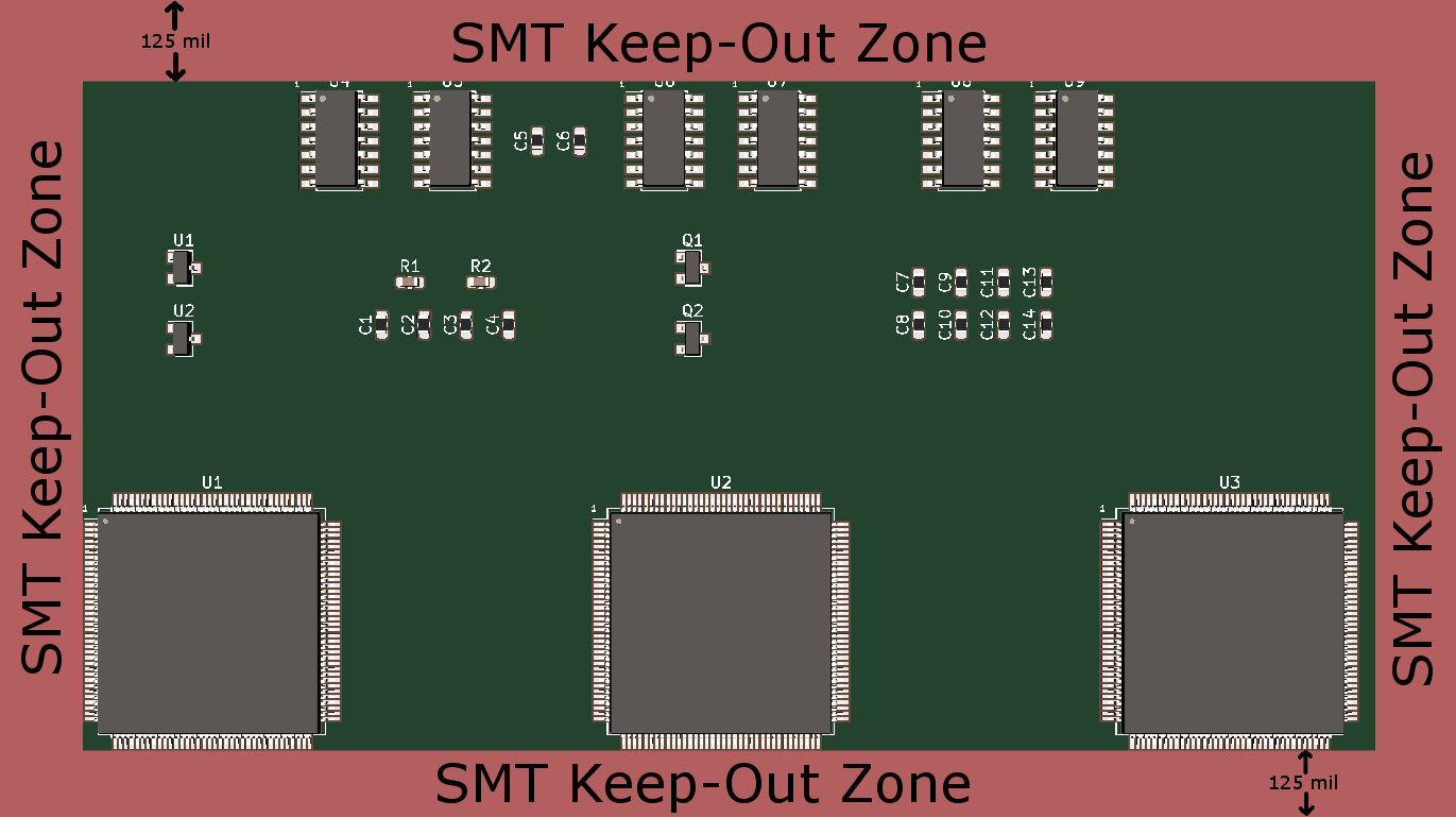
Part-to-board edge spacing for any components on the secondary side of the PCB should be increased to 300 mil. The greater requirement in this case stems from the solder paste screening process, which requires that hold-downs be applied to the secondary side to prevent the PCB from moving while solder paste is applied. Any surface-mount components in this area could be damaged by the hold-downs, or simply blocked during the screening process and left with insufficient solder paste.
It should be specifically noted that the above specifications refer to component pads and bodies for those parts installed by automated assembly processes. Manually assembled parts may be placed closer to the board edge since they can be installed after reflow and depanelization. Copper traces can also be run much closer to the board edge. Both copper traces and manually installed parts should still be kept at least 10 mil from the board edge to allow a solder mask gap and prevent encroachment of the pads.
Some designs require copper plating or castellated holes at the board edge itself. Bittele can handle these requirements, but clients should be advised that the controls involved to produce such PCBs reliably will introduce additional cost and lead time to a project.
Part-to-Hole Spacing
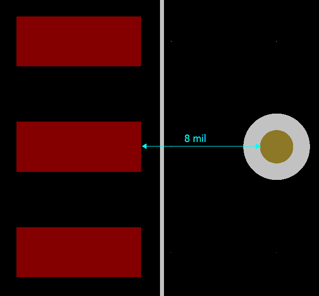
Part-to-hole spacing applies to both through-hole components and PCB vias; it stipulates the minimum spacing required between a component pad or body and either of these types of holes. This spacing is actually divided into two specific parameters, and both of these must be satisfied in order to assure a quality assembly.
- Part-to-Hole Wall: Measured from the edge of the actual hole in the PCB to the edge of a pad. Bittele’s minimum requirement for part-to-hole-wall spacing is 8 mil
- Part-to-Annular Ring: Measured from the edge of the hole’s annular ring to the edge of a pad. Bittele’s minimum requirement for part-to-annular ring spacing is 7 mil

This distinction is drawn because minimum annular ring size and minimum hole size are not proportional, so it is important to ensure that both of these conditions are met during the design phase. For more information on minimum annular ring and minimum hole sizes, see Bittele’s DFM Guidelines.
One last note on this topic is that it is generally a bad idea to place a via between two surface-mount pads, even if Bittele’s minimum part-to-hole spacing is satisfied. This sort of arrangement increases the likelihood of a solder bridge forming under the component during reflow.
Vias placed underneath a QFP or QFN package are less problematic, but should still be avoided if at all possible for maximum quality and yield.
If you still find yourself with any questions about the spacing on your board, please feel free to Contact Us any time! You can reach Bittele via email at sales@7pcb.com, or toll free at 1-888-812-1949.
Related Articles:
Please briefly describe the information you are seeking in the search bar below.