


 English
TURN-KEY PCB ASSEMBLY: BITTELE ELECTRONICS
PCB MANUFACTURING AND ASSEMBLY
Full Turn-Key PCB Manufacturer
You can quickly get quotes and order PCB fabrication and assembly using our online system. Take advantage of exclusive automatic discounts with our tool. Our BOM pricing tool ensures you receive the lowest price for your order.
START A TURN-KEY PCB ORDER
Via in Pad Guidelines
Vias — many people would place them the simplest aspects of a PCB design, but in the world of PCB Fabrication and PCB Assembly, no element can be neglected, and even the simplest of things can get complicated. A prime example of this fact is the case of vias placed within pads for SMT Assembly, which is commonly known as “Via in Pad” design. Via in Pad is a complex process that many manufacturers simply cannot accommodate, but Bittele Electronics is here to help. Our state of the art fabrication and assembly technology, along with our flexible PCB Assembly Process allows us to offer Via in Pad assembly without any risk of compromising the high standard of quality we always provide to our clients.
The first question to ask about Via in Pad is why you might want it in your design, if it can cause so much complication? There are in fact a few cases where this technology does make more sense than any other alternative:
- Spacing concerns for HDI PCBs, or with very fine pitch or high-pin-count BGAs
- Grounding for High-Speed PCB parts in High-Frequency PCB designs
- Improved heat dissipation in thermally sensitive High Power PCB designs
For these reasons, Via in Pad technology might be your only option, and it is sometimes even recommended by part manufacturers. That being said, this process does require more attention during both the fabrication and assembly processes, and thus can cause an increase to the overall cost and PCB Turnaround Time for your project. Here we’ll discuss the appropriate Design for Manufacturing and Design for Assembly techniques to minimize the overall impact of Via in Pad for your PCB.
In order to design around Via in Pad, we should look at just how this technology affects PCB production. The issues of Via in Pad stem from a capillary action that is created by the via hole within the SMT pad. During the Reflow Soldering process, solder tends to be wicked away from the pad itself and down into the via hole.
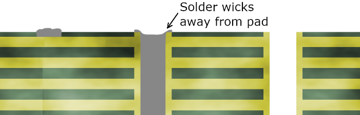
This action can create all sorts of trouble for PCB Assembly, such as Joint Voiding and Cold Solder Defects, or uneven planar surfaces in SMT pads, which are particularly troublesome for BGA Assembly.
The first DFM / DFA advice for those considering Via in Pad is to consider whether or not it is absolutely necessary in your project. Most of the time, other alternatives such as the widely used Dog-Bone Fanout will be more economically viable, even if it means a slight increase to the size of your board.
If other methods just won’t do, then our general advice is to keep the number of Via in Pad instances to a minimum, make the vias themselves as small in diameter as possible, and use Blind Vias to reduce the overall capillary action.
Next, we’ll take a closer look at Via in Pad in specific cases. We’ll talk about how Bittele handles these cases, and when to expect an impact on your PCB Fabrication Quote.
Via in Pad for BGAs and Other Small Pads
For SMT pads with a surface area equal to or less than 0.8 x 0.8 mm, the risk of assembly defects due to Via in Pad capillary action is very high. This is generally true for any BGA, uBGA, POP, LGA, CSP, and other complex package types beyond QFP and QFN (see the following section). Our first advice here is to avoid this type of Via in Pad entirely, if at all possible, as it will unavoidably complicate your project’s assembly. Designing Blind Vias rather than through-hole in these positions can also avoid Via in Pad concerns. Still, if size constraints of your board or component don’t leave any other choice, we can help.
In order to prevent solder from wicking down the via hole, we fill the hole itself with epoxy and cap it with copper plating. The plating prevents any solder from wicking down the pad, while still maintaining electrical and thermal conductivity to the vias internal plating. The epoxy fill adds mechanical strength to the arrangement, to maintain flatness of the pad, and protects against damage that can occur when air trapped in a via expands during reflow. We generally use an epoxy with high thermal conductivity and low electrical conductivity, since the copper plating of the cap and hole offers more than enough current-carrying capability.
This process takes quite a bit of additional effort, especially for PCB designs that incorporate a large number of vias in smaller SMT pads. If your project requires this sort of special attention, you should expect an additional 3-4 days of lead time, and a price increase of roughly 20 – 30 percent, compared to the same board without Via in Pad filling requirements. The specific lead time and cost impact of Via in Pad is project specific, so be sure to talk to one of Bittele’s PCB Customer Service Experts for a more definite estimate of your specific project.
Via in Pad for QFN Thermal Dissipation and Other Large Pads
Thermal pads, especially in QFN Packages, are probably the most common instance of Via in Pad being recommended by part manufacturers. In these cases, the Via in Pad technology is used to improve thermal conductivity away from the part to help with cooling. These pads are normally connected directly to the ground plane of the PCB since it has a relatively large surface area, allowing for considerable heat sinking away from your critical components.
With power demands continuing to increase year-after-year as component sizes progressively shrink, manufacturers see Via in Pad as a convenient way to improve the thermal management of their parts. As such, thermal vias are often factored into the manufacturer’s calculation of thermal characteristics as listed on the part’s datasheet, leaving PCB layout designers no choice but to include these vias on their boards.
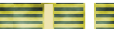
Via in Pad is so commonly recommended in these sorts of parts, that many standard footprint libraries in CAD software include options for QFN and QFP parts that incorporate thermal vias. The image on the right shows one such footprint.
The good news here is that these sorts of vias are of little to no trouble for us at Bittele, and you aren’t likely to see any negative impact for including thermal vias on your QFN parts. For large pads like these, we can cap your vias with solder mask to avoid concerns around capillary action. Unfortunately, this solution is not particularly viable for smaller pads, such as BGA packages, as described above.

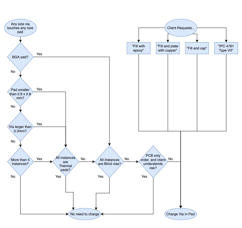
Will Your Vias Cause Trouble?
At this point, you might be wondering if the vias in your design will result in any additional cost or lead time. For a quick summary of the conditions mentioned above, you can refer to the handy flowchart included below.
Related Articles:
Please briefly describe the information you are seeking in the search bar below.