


 English
TURN-KEY PCB ASSEMBLY: BITTELE ELECTRONICS
PCB MANUFACTURING AND ASSEMBLY
Full Turn-Key PCB Manufacturer
You can quickly get quotes and order PCB fabrication and assembly using our online system. Take advantage of exclusive automatic discounts with our tool. Our BOM pricing tool ensures you receive the lowest price for your order.
START A TURN-KEY PCB ORDER
Difference Between Via Tenting and Via in Pad
Vias – they exist in practically every PCB design, and many designers see them as a fairly simple, straightforward aspect of the board. Innocuous as they may seem, in certain circumstances, vias can add a considerable amount of complexity to the PCB Assembly Process. There are a number of different circumstances in which the vias on your PCB might require additional attention, so in this article we will discuss a few different via-related options, and the instances where they might be used.
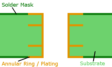
Via Tenting
Bittele only performs Via Tenting upon client request. There is generally no added cost or lead time requirement for this process, and it is normally used simply to prevent accidental contact between the annular rings of the vias and any other circuit elements.
It should be noted that, while via tenting does often close up smaller (less than 12 mil diameter) via holes, this is not the primary purpose of the tenting process; larger holes will not always be entirely sealed.
If you require via tenting on your PCB, simply remove the solder mask clearances from your design, and make a fabrication note to let Bittele know that this was done intentionally. Simply noting that via tenting is expected for this board will let our DFM engineers know that they do not need to contact you for confirmation when they notice the lack of solder mask clearance on your vias.
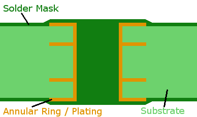
Vias Plugged with Solder Mask
This requirement is most common for BGA packages, where vias are placed very close to the pads of the part in a standard Dog-Bone Fanout. There is a concern in these cases that some solder will be wicked away from nearby pads during assembly, and flow into the open via, resulting in poor connectivity for the BGA part. In order to protect against this issue, the vias can be entirely filled with solder mask.
There is generally no additional cost for this method of filling vias, but there are limitations around when it can be used, which are discussed in the next section, below. When you send your PCB Design Files to Bittele for quotation, our PCB experts will determine whether or not the vias for your BGAs require plugging, and whether or not solder mask can be used.
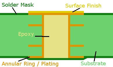
Via in Pad
The final type of via filling is known as Via in Pad, and as the name implies, it refers primarily to cases where the via is placed entirely within the pad of a surface mount component. Many PCB designers taking advantage of this process more than ever before, with increasing difficulty to escape traces since the BGA packages are getting increasingly smaller.
In the solder mask filling process, there was a concern that nearby vias might wick away some solder from a pad, so of course this is an even greater concern when the via is within the pad itself. Solder mask cannot be used for filling since removing solder mask clearance from the SMT pad would make it un-solderable. In this case, Bittele’s production team will fill each via with an epoxy before the surface finish is applied, which requires some additional cost and lead time compared to standard vias.
The epoxy is most often a non-conductive substance, since conductive substances expand much more quickly with heat, which can be troublesome during the reflow soldering process. Non-conductive fill does not impede the via’s ability to conduct electrical current, since the walls are still plated with copper just like any other via. In cases where the via must carry a lot of current or heat through the board, conductive epoxies are available as well.
When you send your design files to us for quotation, it would be helpful to note the presence of any vias within component pads. These will be taken into account for the pricing and lead time you see on your quote, and your account manager can help you to determine if specific vias on your board will require filling of any kind.
Hopefully, this clears up any questions you might have about the different types of attention we might need to pay to your vias during PCB Fabrication. If you find yourself with anything else to ask, we would be happy to chat with you about it! You can reach one of our PCB experts over email at sales@7pcb.com, or toll-free at 1-888-812-1949.
Related Articles:
Please briefly describe the information you are seeking in the search bar below.