


 English
TURN-KEY PCB ASSEMBLY: BITTELE ELECTRONICS
PCB MANUFACTURING AND ASSEMBLY
Full Turn-Key PCB Manufacturer
You can quickly get quotes and order PCB fabrication and assembly using our online system. Take advantage of exclusive automatic discounts with our tool. Our BOM pricing tool ensures you receive the lowest price for your order.
START A TURN-KEY PCB ORDER
Stencil aperture considerations for QFN chips
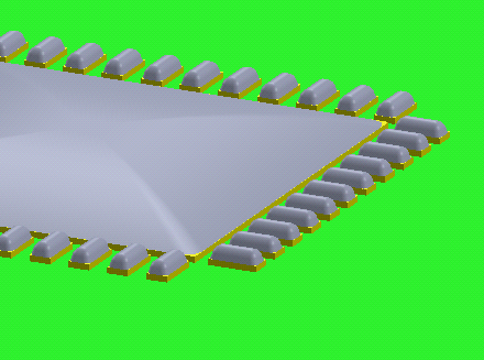
Quad-flat no-leads (QFN), a type of Flat no-leads package, is a surface-mount technology that connects ICs to the surface of PCBs. They have become more popular because of their near chip scale size. Designers can shrink PCB board sizes significantly because QFNs support small form factor and high density packaging and interconnection specifications.
Flat no-leads packages, such as a dual-flat no-leads (DFN), micro leadframe (MLF) and small-outline no leads (SON), are similar in package size to a QFN, but these ICs have exposed thermal pads in their center area. During reflow assembly, these ICs sometimes float on a pool of molten solder located under their thermal pads, which can prevent their terminals from being in contact with the PCB.
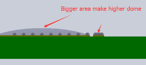
Reflow assembly -- when the board temperature is above the solder’s melting point, the solder paste will liquidate and form a dome-like solder drop due to liquid tension.
A larger amount of solder paste will cover a larger area than a smaller amount. As a result, the larger area of solder paste will create a higher dome than a smaller area due to liquid tension.
The floating solder will lift the ICs. This condition can potentially prevent contact between the ICs' terminals and the PCB pads.
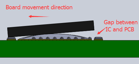
Without any paste volume control during the reflow process, one side of an IC may connect to the PCB pads while the other side may have poor contact due to the excess solder in the center of the thermal pads.
Stencil aperture size must be considered in order to control the solder paste volume in the center of the thermal pads.
Related Articles:
Please briefly describe the information you are seeking in the search bar below.