


 English
TURN-KEY PCB ASSEMBLY: BITTELE ELECTRONICS
PCB MANUFACTURING AND ASSEMBLY
Full Turn-Key PCB Manufacturer
You can quickly get quotes and order PCB fabrication and assembly using our online system. Take advantage of exclusive automatic discounts with our tool. Our BOM pricing tool ensures you receive the lowest price for your order.
START A TURN-KEY PCB ORDER
PCB Outline Layer And Keep-out Polygon Clearance
PCB designers must be diligent about their outline layers and their keep-out clearance. Much thought must be put into this because many problems can arise from neglecting these details.
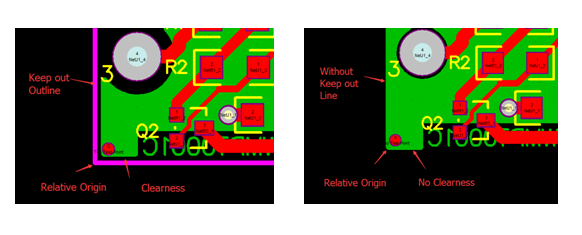
It is very important that the outline layer, also known as the keep-out layer, be present in the Gerber files when manufacturing PCBs. If the designer omits these details, it is likely that they will create an origin point error because the CAM engineer has to get that data indirectly. Furthermore, there will be problems when the boards are panelized.
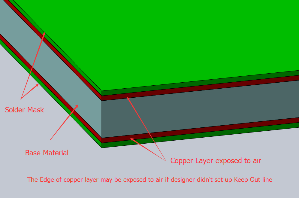
Another problem, if the designer wants to pour the copper polygon over the board, is that the copper at the edge of the board will be exposed to the air. This will increase the likelihood of short circuits when the board goes through the wave soldering process. The molten solder will splash the edge of the board while it is going through the solder pot. Solder will stick to the edge of the board and make solder bridges between the top and bottom copper layers.
At Bittele Electronics Inc., we suggest that the copper polygon must be kept more than 0.2mm away from edge of the board. This is because when we do V-Scoring it leaves a 0.2mm wide groove in the panel. Any copper traces within 0.2mm of the edge of the PCB will be exposed. To ensure safety and proper electrical isolation, we suggest an even greater clearance for high voltage circuits where the supply nears the breakdown voltage of the dielectric.
Related Articles:
Please briefly describe the information you are seeking in the search bar below.