


 English
TURN-KEY PCB ASSEMBLY: BITTELE ELECTRONICS
PCB MANUFACTURING AND ASSEMBLY
Full Turn-Key PCB Manufacturer
You can quickly get quotes and order PCB fabrication and assembly using our online system. Take advantage of exclusive automatic discounts with our tool. Our BOM pricing tool ensures you receive the lowest price for your order.
START A TURN-KEY PCB ORDER
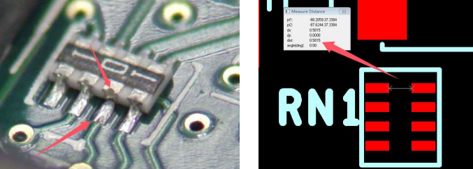
Open Solder Joints in Chip Resistor Array
Defect Description
An open solder joint occurs when solder on the PCB pad fails of proper wetting to the component terminal, resulting in an open solder joint after cooling. See Figure1 for an example.
Root Causes
A. Component Manufacturing Issues
Chip resistor arrays (also known as resistor networks) may develop plating inconsistencies during manufacturing such as electrode "chipping" or insuƯicient electrode coating due to poor process control. This can lead to uneven terminal plating thickness, causing coplanarity issues. Poor coplanarity prevents proper solder wetting at the terminal, resulting in open joints.
B. Placement Misalignment
Improper component placement may prevent terminals to proper contact with the solder paste, leading to poor wetting.
C. Oversized Pad Design
Excessive pad spacing (inner pitch) can prevent solder joint formation eƯectively to the smaller components.
Corrective Actions
1. Process Improvements
- A. Stencil Optimization
Use step-down stencil designs to increase solder paste volume or apply adhesive tape under the stencil to locally increase solder paste thickness. - B. Placement Optimization
Adjust component pick-up centroid and reduce placement speed to ensure proper contact between the component terminals and solder paste on both pads.
2. Design Improvements:
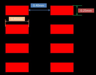
- A. Reduce Pad Spacing
Minimize the pad pitch where possible. For example, reduce from 0.58 mm to 0.4 mm, and narrow the pad width from 0.45 mm to 0.25 mm while keeping the pad length at 0.45 mm as shown in Figure2.
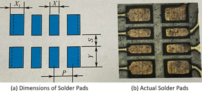
- B. Increase Corner Pad Width
In Figure3, increasing the width of the four corner pads (X1) to enhances surface tension during reflow, helping to self-align the component and improve solder wetting at the inner terminals thereby reducing the risk of open joints.
If you would like to begin the quotation process or learn more about our capabilities, you may contact us at 1-416-800-7540 or by email at sales@7pcb.com to get in touch with one of our PCB specialists.
Related Articles:
Please briefly describe the information you are seeking in the search bar below.