


 English
TURN-KEY PCB ASSEMBLY: BITTELE ELECTRONICS
PCB MANUFACTURING AND ASSEMBLY
Full Turn-Key PCB Manufacturer
You can quickly get quotes and order PCB fabrication and assembly using our online system. Take advantage of exclusive automatic discounts with our tool. Our BOM pricing tool ensures you receive the lowest price for your order.
START A TURN-KEY PCB ORDER
Manufacturing Process of Multilayer Rigid-Flex PCBs
Process Overview
Due to the structural complexity of rigid-flex PCBs, the manufacturing processes can vary depending on the design. Figure1 illustrates a typical rigid-flex stack-up structure using the conventional standard process flow in Figure2. The process begins with the fabrication of double-sided flexible copper-clad laminates.
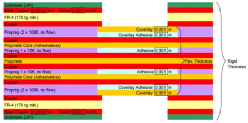
All conductor patterns excluding for plated through-holes are formed using conventional etching techniques. In the flexible areas, conductor layers are laminated with coverlay films that have no openings. While the flexible sub-layers are bonded together using pre-cut adhesive sheets with windowed in the flex zone areas, ensuring they do not interfere with bendability. The rigid outer layers (i.e., the rigid sections on the top and bottom) use double sided rigid copper-clad laminates.
Key Process Steps Used
1. Preparation of Rigid Outer Layers
The process begins with the fabrication of rigid outer layers, which are then laminated onto the inner circuit layers. CNC routing, punching, or laser machining is then used to partially or fully remove the rigid material in the flexible areas. Next, the flexible layers and the machined rigid outer layers are laminated together using adhesive sheets. These adhesives must be pre-cut windows to avoid stiffening the flexible sections.
2. Lamination
During lamination, if the rigid outer layers are recessed or partially routed, suitable pressure relief or filler plates must be used to support uniform pressure over the flex areas. Vacuum lamination is recommended to achieve optimal bond quality and uniform pressure distribution across the panel. Conformal materials (such as PE films) may be used to ensure even pressure and flow during the lamination cycle. Low-flow adhesives are expected to fill voids adequately, particularly in complex stack-ups. Pre-baking of sub-assemblies is necessary to remove residual moisture prior to lamination.
3. Drilling and Hole Preparation
After lamination, the rigid-flex board undergoes through-hole drilling process similar to that conventional multilayer rigid PCBs. However, hole desmearing techniques vary based on the material stack-up. As with rigid boards, holes are drilled after thorough pre baking to eliminate moisture, followed by plasma etching to remove resin smear from the hole walls. The recommended etchback depth is generally no more than 13 µm. Subsequently, the through-holes undergo standard electroplating, although plating parameters should be defined based on reliability test data for via integrity.
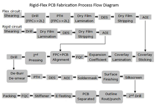
4. Final Board Process
After metallization, the remaining process steps align with those of standard multilayer rigid boards such as outer layer imaging and etching, solder mask (coverlay or LPI application), and Surface finish (ENIG, HASL, etc.). In the final profiling step, any temporary filler plates in the flexible areas or depth-controlled rigid outer layers are removed. This exposes the flex regions and completes the transformation into a fully functional rigid-flex PCB.
Please contact us at any moment to learn more about our capabilities or to submit your PCB design files for a formal quote! You can contact us by phone at 1-416-800-7540 or by email at sales@7pcb.com.
Related Articles:
Please briefly describe the information you are seeking in the search bar below.