


 English
TURN-KEY PCB ASSEMBLY: BITTELE ELECTRONICS
PCB MANUFACTURING AND ASSEMBLY
Full Turn-Key PCB Manufacturer
You can quickly get quotes and order PCB fabrication and assembly using our online system. Take advantage of exclusive automatic discounts with our tool. Our BOM pricing tool ensures you receive the lowest price for your order.
START A TURN-KEY PCB ORDER
Making Readable Silkscreen Layouts for your PCB Design
What is a PCB design silkscreen and why include them in a design plan? What does your PCB need to be a good readable silkscreens?
What are Silkscreens?
Generally a Printed Circuit Board (PCB) Design has many different layers and the silkscreen layer is one of these layers. Since the silkscreen must be printed on the PCB surface there are at most two silkscreen layers the top and bottom for each PCB. Silkscreens holds text information printed onto the board for humans to read and interpret. On the silkscreen of a PCB you may print all sorts of information like the component reference designators, company logos, manufacturer marks, warning symbols, part numbers, version numbers, date code, etc. However space on a PCB’s surface is limited so it is best to limit it to useful or important information. Thus the silkscreen layer usually only holds a component legend showing where the various components go on the board with company logos and board design number.
Currently custom built digtal ink-jet printers specially for printing PCBs are most often used for printing silkscreens images onto PCB surfaces from board design data. Originally silkscreens were printed using the screen printing methods from which the name silkscreen is derived. This name is due to traditional screen printing technique being known for requiring a sheet of fine cloth like silk or polyester as a screen and a frame made of wood, aluminum, etc. Now as technology advanced many different simpler or faster methods for silkscreen printing were developed but the name remained the same.
How to Design Silkscreens?
Notably editing the silkscreen layouts on a PCB design is a minor step in PCB Design since a silkscreen is not necessary for assembling a PCB. However while it is not absolutely necessary step it is still an important step that aids in the assembly of the circuit board by providing references during construction and troubleshooting. Various computer programs for PCB Design are available on the market for example the well known Mentor Graphics PADs Layout and Router. In the case of Mentor Graphics PADs when designing a PCB Layout when placing components on the layout in the design file a component reference designator code is automatically assigned to each component on the layout.
When designing the PCB layout we move and rotate the component on the layout. Component reference designator codes move and rotate with them since they are attached to the components. Thus editing the silkscreen becomes necessary in this case. There are also programs where you design the silkscreen writing the component reference designator codes yourself to go with the corresponding component locations. In these programs you just need to be aware of the key points below while taking care to assign different reference code to each component.
Orientation/Overlaps
Regardless of whether you are editing an automatically generated silkscreen or designing a silkscreen layer from scratch, there are key points that you should pay attention to if you want to design a good readable silkscreen layer design. In order to design a good silkscreen you need to:
- Edit the orientation of text for component reference designator, part type, etc so that all these have the same orientation, if possible setting up a top and bottom which means the silkscreen would be easier to read.
-
Check for overlapping texts before rotating the text and adjusting the component reference designator marks. One example, is shown in Fig.1 below, the marks have different orientations and are overlapping. In the picture you can see how confusing and difficult the marks would be to use as references when assembling or troubleshooting if not corrected. As such you need to rotate and move component reference designator to the correct orientation and positions by the corresponding component.
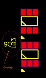
Fig.1 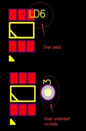
Fig.1 
Fig.1 - Take note that before constructing a circuit board, PCB manufacturers usually automatically trim the component reference designator marks that go over pads and vias to avoid them overlapping and possibly affecting the circuits with:
- Check for component reference designator marks that were put over circuit pads overlapping with the pads like on the first component mark circled in Fig.2 . Since they are usually trimmed out and not printed and you need component reference marks as guides during PCB assembly and troubleshooting you need to move these marks to an open space with a position next to the corresponding component.
- Check for marks over via holes like the one shown beside the second component mark in Fig.2. Since untented via holes do not have a surface to be printed over, you cannot print on it but when you use a tented via where you cover the via hole with solder mask you cannot use it as a test point. Thus if there is space it is best to move it to a position next to the corresponding component.
- Check if there are any reference marks placed so that it would be under objects once the components are soldered on, like in Fig.3, if there are marks under the component, they need to be moved. Since reference marks need to be seen to be of use, when covered by components they are of limited use as references during troubleshooting and PCB assembly.
Additional Marks
-
Adding extra marks may help show the orientation of components on the circuit board like in Fig.4. You may add marks with shapes like triangles, etc in addition to the original orientation signs on the component object marks to help show the orientation of components with different I/Os that need it.
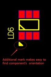
Fig.4 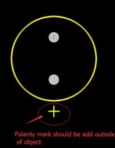
Fig.5 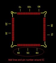
Fig.6 - Place polarity marks like the positive mark in Fig.5 outside of the component object marks. For components like large capacitor or other components with specific polarity it reduces the chances of component orientation mistakes during the board assembly which makes the process much smoother.
- Add measurement marks of the number of pins and lines on a microchips (ICs) on the silkscreen like in Fig.6.
Design Considerations
Other points you may wish to consider when designing a silkscreen is that if you:
- Restrict the silkscreen to only one side like the top may cut your printing cost in half since in that case you would only need to print one side not two. Not true in Bittele’s case we don’t charge anything for single or double sided silkscreen.
- Mark using standard colours and larger shapes makes silkscreen cheaper and easier to read since you need special inks and standard colours are usually in stock thus cheaper than a colour that needs to be special ordered.
- Measure distances to allow a certain amount of tolerance for common printing errors in the board by a few mils difference. Can reduce the possibility of problems due to machine printing errors.
Related Articles:
Please briefly describe the information you are seeking in the search bar below.