


 English
TURN-KEY PCB ASSEMBLY: BITTELE ELECTRONICS
PCB MANUFACTURING AND ASSEMBLY
Full Turn-Key PCB Manufacturer
You can quickly get quotes and order PCB fabrication and assembly using our online system. Take advantage of exclusive automatic discounts with our tool. Our BOM pricing tool ensures you receive the lowest price for your order.
START A TURN-KEY PCB ORDER
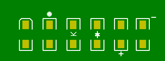
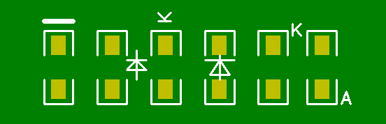
Marking Diode Poles on Silkscreen Layer
Diodes are a type of circuit component which conducts electricity typically in one direction as they have a low resistance in one direction and very high resistance in the other direction. This directionality requires that the component be assembled in a particular orientation in order to operate as intended. To ensure proper installation by your circuit assembler, it is important to include a mark on the silkscreen layer to identify which terminal is the anode and which terminal is the cathode.
However, a board that has a (+) silk screen marking is not enough information to tell the assembly house how to correctly insert a diode because there are different types of diodes. For zener or barrier diodes, the (+) marking may or may not be the cathode of the component. Furthermore, an LED usually has a (+) anode, but not all the time. To verify the proper way to place a diode onto a PCB, it is best to use an “A” for anode or a “K” for cathode (C is used to label capacitors thus to avoid confusion we recommend K for cathode). You may also use a circuit symbol of a diode to show the orientation, however this requires more space on a board than a letter and may not be useful for dense board layouts. See the diagrams below for a comparison between ambiguous and clear diode markings.
By properly labelling your diodes you avoid the need to clarify your design intentions further and reduce the likelihood of diodes being placed incorrectly.
Related Articles:
Please briefly describe the information you are seeking in the search bar below.