TURN-KEY PCB ASSEMBLY: BITTELE ELECTRONICS
PCB MANUFACTURING AND ASSEMBLY
Full Turn-Key PCB Manufacturer
You can quickly get quotes and order PCB fabrication and assembly using our online system. Take advantage of exclusive automatic discounts with our tool. Our BOM pricing tool ensures you receive the lowest price for your order.
START A TURN-KEY PCB ORDER
What are the common defects in PCB manufacturing?
PCB is an important part of electronic products, and its quality directly affects the performance and reliability of the entire product. However, various defects often occur during the production of PCBs, which not only affect the quality and appearance of PCBs, but may also cause circuit function failure or cause other problems.
So, what are the common defects of PCBs? Today we will explain them in detail.
Open and short circuit
Open circuit and short circuit are among the most common defects of PCB boards. An open circuit refers to the lack of connection between two points that should be connected in a circuit, resulting in the inability of current to flow; while a short circuit refers to the presence of a connection between two points that should not be connected in a circuit, resulting in abnormal current flow.
Both defects can cause circuit failure and, in severe cases, damage components.
Pad falling off
Pad shedding refers to the loose welding between the component pins and the PCB pads, causing the pads to fall off the PCB.
This defect can cause an open circuit or component failure, seriously affecting the reliability and service life of the product.
Copper foil warping
Copper foil curling refers to the separation of the copper foil on the PCB from the substrate, causing the copper foil to curl or curl.
This defect will affect the conductivity and appearance quality of the PCB board, and in severe cases may cause the circuit to be open or short-circuited.
The hole wall copper is thin or no copper
Thin copper or no copper on the hole wall means that the copper layer on the inner wall of the via or through-hole of the PCB board is too thin or there is no copper layer.
This defect will cause the circuit conduction performance to deteriorate, and in severe cases may even cause the circuit to open.
Green Oil Bridging and Green Oil Foaming
Green oil bridging refers to the situation where two adjacent pads on the PCB are covered with green oil, resulting in the inability to form an effective soldering point during soldering; while green oil blistering refers to the appearance of bubbles or bulges in the green oil layer on the circuit board.
Both defects will affect welding quality and circuit conductivity.
Line width and spacing do not meet requirements
Line width and spacing that do not meet requirements means that the line width and spacing on the printed circuit board do not meet the design requirements or exceed the allowable range.
This defect will affect the conduction performance and reliability of the circuit, and in severe cases may even cause the circuit to fail.
Solder mask peeling and discoloration
Solder mask peeling refers to the separation or peeling of the solder mask on the printed circuit board from the substrate; while solder mask discoloration refers to the change in color or loss of gloss of the solder mask.
Both defects will affect the appearance quality and welding performance of the PCB board.
Misalignment and delamination of inner layers in multilayer boards
The misalignment of the inner layers of a multi-layer PCB refers to the displacement of the positions of the layers in the multi-layer circuit board; while delamination refers to the separation or cracking of the layers in the multi-layer PCB.
Both defects will affect the conductivity and reliability of multi-layer PCB boards.
Oxidation and contamination
Oxidation and contamination refer to the presence of oxides, stains or other contaminants on the surface of the circuit board.
This defect will affect the conductivity and welding performance of the PCB, and in severe cases may even cause circuit function failure.
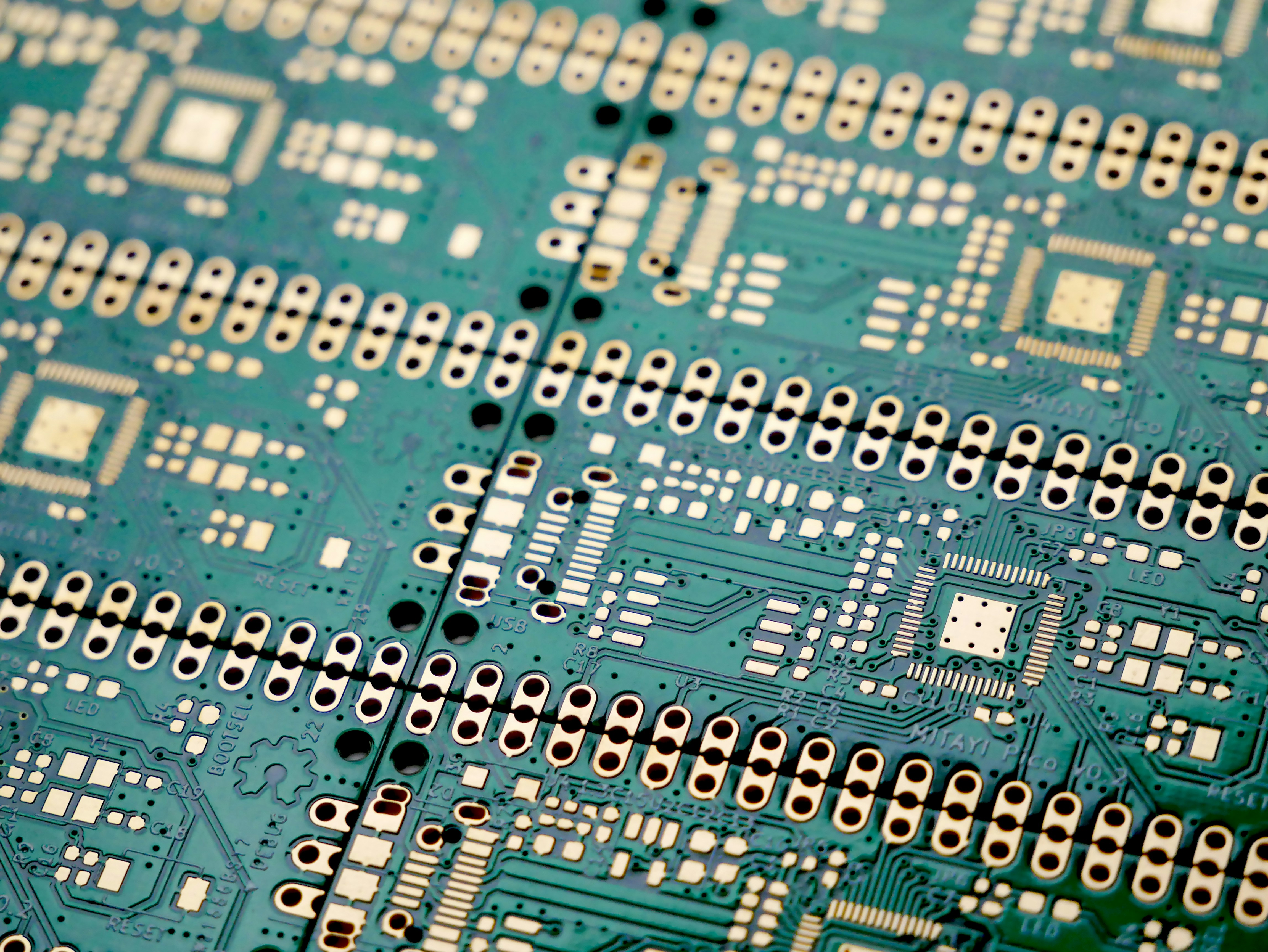
Common defects of circuit cards include open circuits and short circuits, pad shedding, copper foil lift, thin or no copper in the hole wall, green oil bridging and blistering, line width and spacing not meeting requirements, solder mask shedding and discoloration, inner layer misalignment and delamination of multi-layer boards, oxidation and contamination, etc.
In order to avoid these defects, we need to strictly control the manufacturing and assembly of PCB boards, strengthen quality inspection and control, and ensure that each printed circuit board meets the quality requirements.
Related Articles:
- How to Prevent the Tombstone and Open Defects during the SMT Reflow Process
- Which Soldering Defects are Related to the Incorrect Setup of the Reflow Profile?
- How to Prevent Non-Wetting Defect during the SMT Reflow Process
- An Analysis of SMT Solder Paste Printing Defects
- How to Prevent Solder Ball and Bridging Defects during the SMT Reflow Process
Please briefly describe the information you are seeking in the search bar below.






 English