


 English
TURN-KEY PCB ASSEMBLY: BITTELE ELECTRONICS
PCB MANUFACTURING AND ASSEMBLY
Full Turn-Key PCB Manufacturer
You can quickly get quotes and order PCB fabrication and assembly using our online system. Take advantage of exclusive automatic discounts with our tool. Our BOM pricing tool ensures you receive the lowest price for your order.
START A TURN-KEY PCB ORDER
PCB Assembly Process
At Bittele Electronics, we pride ourselves on our efficient and high-quality turnkey PCB assembly service. Bittele employs a number of strategies in Quality Management and process control to ensure that every PCB order is done right the first time. In order to achieve the fastest possible turnaround of the highest quality product, we continuously strive to improve our services and to make each step as efficient as possible.
This article provides a step-by-step overview of the standard turnkey PCB assembly process, providing key information at each stage that might relate to a client’s interest. This is a brief overview only, and for those interested in a more detailed elaboration around Bittele’s specific capabilities, we recommend reading our comprehensive DFM Guidelines and DFA Guidelines documents.
One of the most important factors in the overall efficiency of each PCB assembly project is the client’s understanding of Bittele’s process. The number of steps involved in the PCB assembly process depends upon the specific nature of the project in question, as illustrated by the flowchart below, and each of these steps is explained briefly in the following sections. For simplicity’s sake, some intermediary stages are not shown in this flowchart; for example, each stage includes individual inspection upon completion. By being acquainted with this process, a clever engineer can create a PCB precisely for a quick and economical process by reducing the total number of tasks needed.
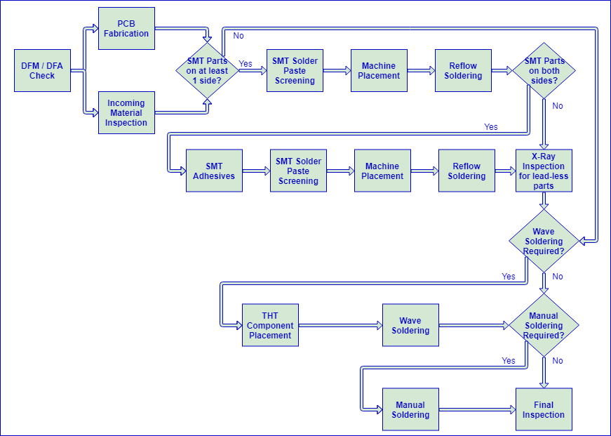
DFM / DFA Check
Once a turnkey order is released to Bittele’s production team, their very first task is the validate the design through a thorough DFM / DFA Check process. These checks include verification of consistency across different design documents (i.e. BoM, Gerbers, Centroid, etc.), part spacing, footprint accuracy, and clear orientation markings. The main objective of this procedure is to minimize as much as possible the potential for design errors to affect the finished product, which acts to protect Bittele’s clients against the additional time and cost involved with board-level rework.
Customers should look for emails from Bittele's production department, which is sent out between one and two days after an order is submitted. If any problems or inaccuracies are found during our initial check, our production coordinator responsible for your order will contact you directly for solution. Typically, a detailed report will be sent to you for a reply, and the order will be put on hold awaiting complete confirmation, hence, it's essential to respond to our questions as soon as you can to prevent any work stoppages.
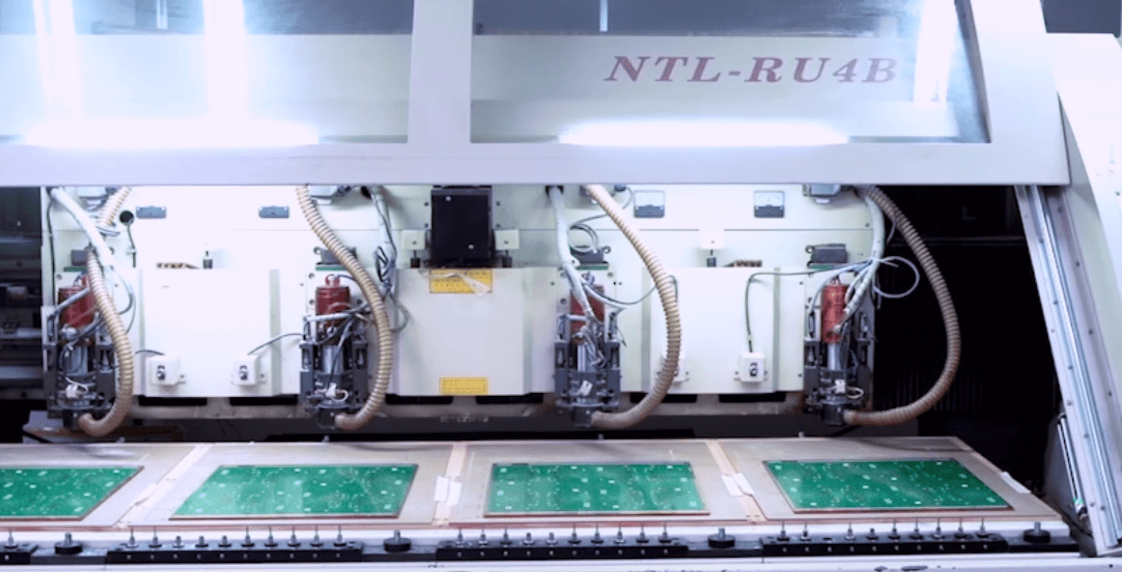
PCB Fabrication
Once the initial DFM / DFA Check is complete, the order proceeds to the PCB Fabrication stage. Here the bare PCB is formed through multiple stages of Material Lamination, Drilling and Copper Deposition / Etching, depending upon the design requirements; the stencil for solder paste screening (discussed below) is also created during this stage. The Solder Mask and Surface Finish, which aid in PCB assembly, are then added to the board, and finally, the Silkscreen is printed over all. Once the boards are fully formed, Electrical Testing is conducted against a client’s Netlist file, to verify 100% conformance with design requirements. Finally, Tab Routing or V-Scoring defines the profile of each individual PCB within the fabricated panel, providing for ease of separation after PCB Assembly is completed.
As the focus of this article is the PCB Assembly Process, the above is only a brief overview of PCB Fabrication, which is an intricate process in its own right. For a comprehensive discussion of Bittele’s process and capabilities regarding PCB Fabrication, please see our DFM Guidelines document.
Incoming Material Inspection
Bittele’s Parts Procurement team works concurrently with our PCB Fabrication team to ensure that all assembly materials are received and ready for use as soon as the bare PCBs are ready for assembly. As parts are received at Bittele’s production facility, our Incoming Quality Control (IQC) team conducts a thorough inspection before warehousing any particular material or component. Inspections include sample operational testing as well as date code verification and entry into a software material management system. Our sophisticated software management system ensures that rules of first-in-first-out are strictly followed, and that parts used in PCB Assembly are always in good working order.
The combined efforts of Bittele’s IQC and Parts Procurement teams ensure that all parts used in PCB assembly are of the highest quality so that our clients can be confident in the overall shelf-life of their products.
SMT Solder Paste Screening
The first step in the actual PCB Assembly process is the application of solder paste to the bare PCBs. Here the stainless-steel stencil that was created during PCB Fabrication is fit over the bare board, leaving only the pads for assembly of surface-mount components uncovered. The stencil is held in place by a mechanical fixture, and an applicator moves over the surface of the board to meticulously distribute solder paste over those uncovered spaces. Bittele’s quality control team then performs a thorough inspection to ensure that the solder has only been applied to the necessary areas, and that all pads are covered with a sufficient amount of paste. For double-sided SMT boards, this process will need to be performed individually for each side, as indicated in the above flowchart.
Bittele’s solder of choice is SAC305, which is a Lead-Free alloy containing 96.5% tin, 3% silver, and 0.5% copper, and is compliant with the RoHS, REACH, and JEIDA directives. We use the paste version of this material for reflow soldering, and solid versions for manual and wave soldering.
Machine Placement
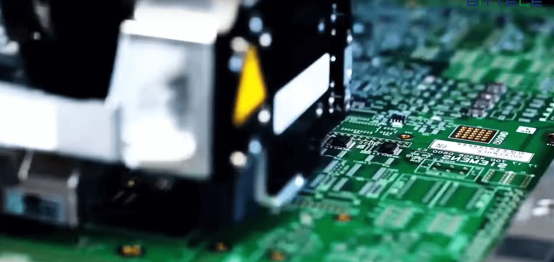
Once solder paste is applied to the bare PCBs, they are moved to Bittele’s automated Pick & Place machines for the actual mounting of components on their associated pads. Part placement is 100% machine automated for maximum accuracy and efficiency, and uses the project’s Centroid file for component coordinates and rotation data. The boards are again inspected after components have been mounted to ensure all placements are accurate before the soldering process begins.
This stage might need to be performed multiple times, depending upon the specifics of a given project. Double-sided SMT boards require one round of placement for the top and one for the bottom, and projects requiring wave soldering due to a high number of through-hole parts will normally have their components machine-placed as well.
Reflow Soldering
With parts mounted securely in place with solder paste underneath their pads, it is time for the PCBs to enter the reflow soldering phase. This is the most common method for PCB assembly in the industry today since it is much more flexible in terms of PCB layout requirements compared with wave or manual soldering. Most of the time, Bittele can use reflow soldering for a majority of the components on a board, and then pass the mostly-assembled boards to our highly skilled manual soldering team for the final few connectors.
For a double-sided SMT order, it’s required that the PCBs be reflowed separately for each side. An appropriate adhesive is applied beneath the parts that were soldered during the first production run to avoid having them loosen and separate from the PCB when their solder is re-heated.
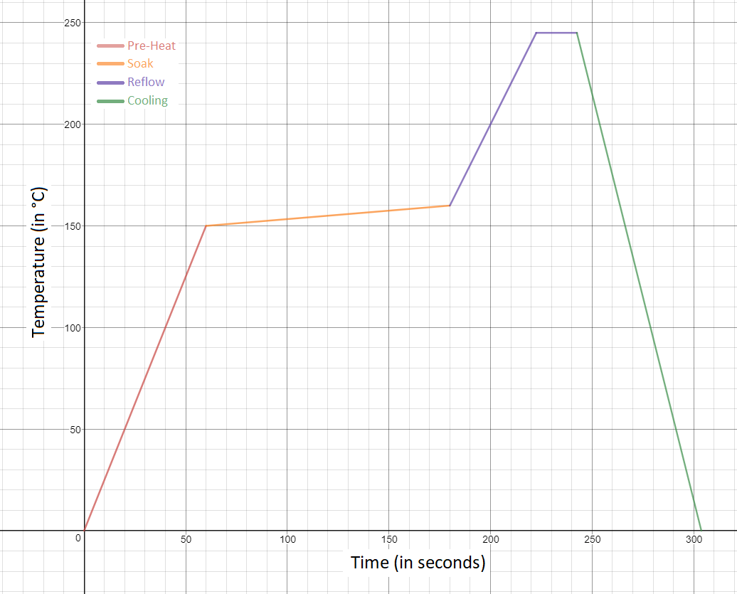
The primary issue in reflow soldering is that the part must be able to handle elevated temperatures for a longer time than would be necessary for either wave or manual soldering. Most of today's SMT components are developed for these thermal profiles, but a large number of THT components are incompatible with reflow soldering for this requirement. Bittele’s standard reflow cycle is described by the graph below.
| Pre-heat | to 150 °C | in 60 seconds |
| Soak | from 150 °C to 165 °C | in 120 seconds |
| Reflow | Peak temperature 245 °C | hold for 20 seconds |
| Cooling | –4 °C per second | to room temperature |
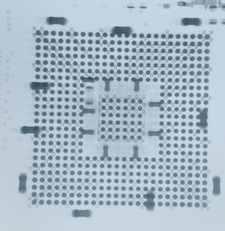
X-Ray Inspection
After a reflow cycle, any boards including BGA, QFN, or other lead-less package types are sent for X-Ray Inspection; this service is included by default on all Bittele quotations which include such parts.
X-Rays penetrate the silicon of an IC package and reflect from the metal connections underneath, forming an image of the solder joints themselves that can be analyzed by advanced image processing software similar to Automated Optical Inspection (AOI). Higher-density features in the captured area create a darker resulting image, allowing for quantitative analysis to determine quality of the solder joints and compare against industry standards.
Not only does X-Ray inspection detect issues in PCB assembly, but the analysis of an X-Ray image can help to determine the root cause of a given defect, such as insufficient solder paste, skewed part placement, or improper reflow profile.
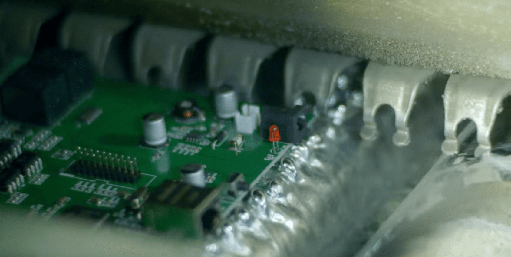
Wave Soldering
Wave soldering is a method of PCB Assembly that involves sending boards on a conveyor through a “wave” of molten solder. The solder bonds together exposed component pads and leads while wicking off of the bodies of components and the solder masked bulk of the board.
Wave soldering has fallen somewhat out of favour in the PCB assembly industry in recent years, at least in comparison to its past prevalence. The growing popularity of surface mount parts and High-Density Interconnect (HDI) PCB layouts make reflow soldering the method of choice for a majority of projects, and manual soldering can be used to take care of the typically few components not suitable for reflow. That being said, wave soldering certainly still has its place. For legacy boards requiring high proportions of Through-Hole Assembly, as well as boards incorporating large connectors with very high pin counts, wave soldering is often still the most efficient method for PCB assembly.
Bittele would recommend that clients design for reflow soldering as often as possible since wave soldering does require more strict controls in design than reflow soldering. Bittele’s process engineering team performs a thorough analysis of the PCB design before any wave soldering job, and will bring up any potential complications with a client in advance, but this does require additional time and cost compared to a reflow soldering project.
Manual Soldering
Manual soldering is generally used when a PCB design incorporates some parts that are not suitable for either reflow or wave soldering. For example, a majority surface mount PCB might include a few through-hole components, and wave soldering these few parts would unnecessarily drive up the cost of production. Bittele employs a staff of highly skilled manual soldering specialists to take care of any such requirements, who provide consistent and reliable workmanship even up to IPC-A-610 Class 3 Standards.
While Bittele’s manual soldering specialists are incredibly proficient at their tasks, they are still subject to certain human limitations that do not apply to automated assembly methods. The most common manual assembly restrictions are listed below:
- Multiple-row connectors (more than 2 rows) cannot be manually soldered since the tip of a soldering iron will not fit between rows; these devices are usually wave soldered
- BGA, QFN, and other lead-less packages cannot be manually soldered
- Part-to-Part Spacing* and Part-to-Hole Spacing* requirements must be carefully observed, and an additional margin of 5 to 10 mil is recommended around any manual assembly parts
- Pad and Hole Size* requirements must be strictly followed, and an additional margin of 10% is strongly recommended for the SMT pad-to-lead ratio of manual assembly parts
*For spacing and sizing requirements, see Bittele’s DFA Guidelines document
Final Inspection
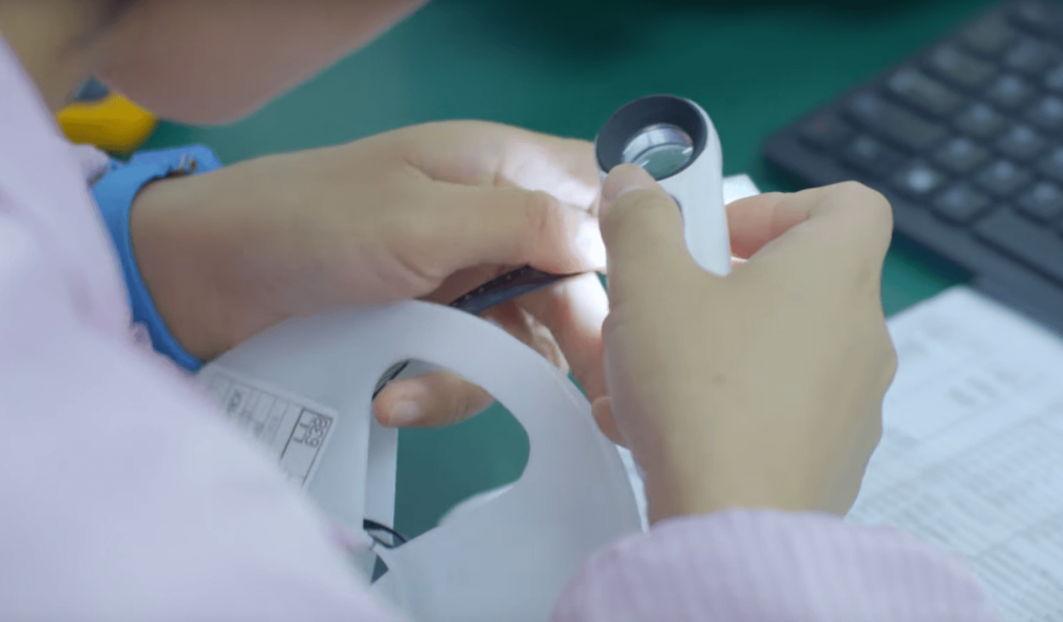
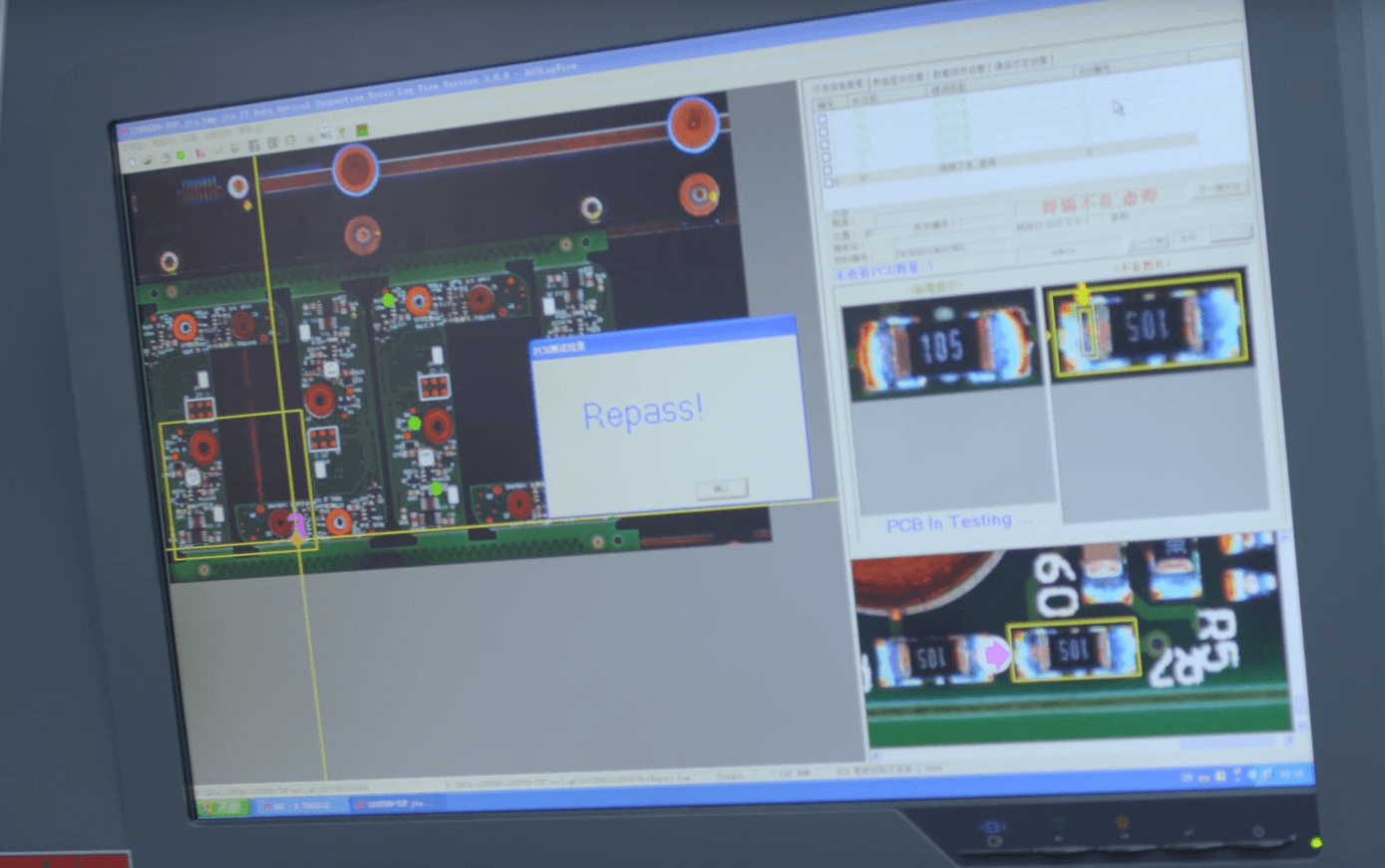
As noted above, inspections are carried out after every individual stage of the PCB assembly process to better localize the source of any error. Bittele views these intermediary inspections necessary but not sufficient to fully guarantee the highest in quality of workmanship, as is our mission, and as such we always perform a thorough final inspection on the fully finished boards at the end of the process.
These final inspections always include visual inspection by Bittele’s highly experienced quality assurance team, and Automated Optical Inspection (AOI) for complex or high-volume projects. We can also provide additional services such as Functional Circuit Testing (FCT) and In-Circuit Testing (ICT) upon client request. The more involved testing methods of ICT and FCT will require some additional lead time and labour cost depending upon the specific requirements for a given project, but can relieve the need for involved product testing on the client end.
Industry-Leading PCB Assembly Experts
Bittele has been offering professional PCB Assembly services since 2003, and we have refined our process over the years to ensure that our clients get the best possible value on every project. Our meticulous process meets the industry’s most stringent standards, including ISO-9001:2008, IPC Class 3, and RoHS. A partnership with Bittele offers full confidence that your PCB project will be carried out with the very best in quality control, efficiency, flexibility, and customer service.
We can handle designs and requirements of all types, and we encourage prospective clients to get in touch with us for any questions that might not be captured in this brief overview. You can Contact Us by email at sales@7pcb.com, by toll-free telephone at 1-888-812-1949, or using our 24-hour Live Chat available on our website at www.7pcb.com.