


 English
TURN-KEY PCB ASSEMBLY: BITTELE ELECTRONICS
PCB MANUFACTURING AND ASSEMBLY
Full Turn-Key PCB Manufacturer
You can quickly get quotes and order PCB fabrication and assembly using our online system. Take advantage of exclusive automatic discounts with our tool. Our BOM pricing tool ensures you receive the lowest price for your order.
START A TURN-KEY PCB ORDER
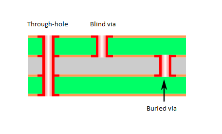
Working with Blind and Buried Vias
Bittele uses blind and buried vias in the production of high-density interconnect (HDI) PCBs. As opposed to a typical plated through-hole via, blind and buried vias do not travel through the board from top to bottom. Instead, blind vias connect any one of the external layers of a multi-layer PCB to an internal layer within the dielectric substrate, while buried vias connect each internal layer to the other.
What Makes Blind and Buried Vias Important?
The complexity of a multi-layer HDI circuit board is dictated by the physical dimensions of the design, and the number of SMT components on both external layers (especially ICs with QFN, BGA and fine-pitch footprints). As such components would interfere with a designer’s ability to pass tracks under them, multi-layered circuit design should be considered. The dimensions and placement of each blind and buried via is critical, due to both PCB real estate constraints and power/signal delivery within the circuit.
Other considerations include which layers each via will connect to, whether they will intersect with each other and whether any through-hole components will be fitted into a blind via. Please refer to our DFM and DFA guidelines for more information.
What are Intersected Blind and Buried Vias?
Blind and buried vias are said to intersect, under the following conditions:
- If two or more vias pass through a minimum of 2 layers in the PCB
- If each via contacts a minimum of 1 common layer
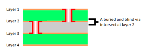
In the above example, a four-layered PCB has one blind via connecting layers 1 and 2. A buried via connects layers 2 and 3. Since both vias pass through 2 layers, and since both vias make contact with layer 2, the two vias are considered intersected.
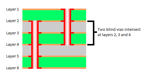
In this example, a six-layered PCB has one blind via connecting layers 1 to 2, 3 and 4. A second blind via connects layers 6 to 5, 4, 3 and 2. Since both vias pass through more than 2 layers, and since both vias make contact with layers 2, 3 and 4, the two vias are considered intersected.
Is it Possible to Solder Through-Hole Parts into Blind Vias?
Soldering through-hole components into blind vias is both possible and a viable solution to space-constrained PCBs. When designing HDI circuits, we understand how critical real estate can be on a crowded board. Our support team is very eager to advise you on improving the efficiency of your PCB design, in your search for reduced costs and high quality HDI circuit production.
What Options Exist for Protecting Blind and Buried Vias?
As with through-hole vias, epoxy is typically filled into blind and buried vias, to protect them from the elements and give the PCB mechanical reinforcement. However, depending on your design needs, blind vias can also be tented (covered) in solder mask to protect them from short circuits, or left untreated in order to accept through-hole components. We can accommodate any special design needs and our support team is very eager to assist you.
What are the Biggest and Smallest Diameters of Drill Holes for Blind and Buried Vias?
Typical drill hole diameters range from 6 mils to 24 mils, which can be achieved with mechanical drilling techniques. However, we can achieve vias as small as 3 mils in diameter, thanks to our state-of-the-art laser drilling techniques. As to which drilling option and dimensions fit best for your design, our support team is more than happy to assist you with your DFM needs.
Related Articles:
Please briefly describe the information you are seeking in the search bar below.