


 English
TURN-KEY PCB ASSEMBLY: BITTELE ELECTRONICS
PCB MANUFACTURING AND ASSEMBLY
Full Turn-Key PCB Manufacturer
You can quickly get quotes and order PCB fabrication and assembly using our online system. Take advantage of exclusive automatic discounts with our tool. Our BOM pricing tool ensures you receive the lowest price for your order.
START A TURN-KEY PCB ORDER
Tailoring Your CAD PCB Design Rules to Our Capabilities
The Design Rule Check (DRC) feature of your PCB CAD software helps to ensure that your design is well-suited for PCB Fabrication and PCB Assembly. In order to get the most out of this feature, you will need to set it up according to Bittele’s specific manufacturing specifications. Constraining your design within our capabilities will make for a more efficient PCB Assembly Process, by reducing the amount of time required for questions and potential changes during the quotation and DFM Validation stages of the project. This article gives a brief overview of our key design rules, and outlines the process for updating them in a few common CAD PCB layout software packages. For a complete picture of our capabilities, please see our comprehensive DFM Guidelines and DFA Guidelines documents.
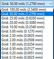
The first step in setting up your Bittele-specific design rules is to set the grid for your design. We strongly recommend that parts be placed exclusively using a 50 mil (1.27 mm) grid. This sort of consistency helps to promote Proper PCB Component Alignment, allowing for a more efficient Automated Assembly Process via Bittele’s Pick & Place machines.
With your grid size properly defined, the next step is to open up the Design Rules Editor in your CAD layout software of choice. There are many available software packages on the market, so your view might look slightly different than what you see here, but any PCB layout software worth its salt will have an interface for editing design rules.
First, we set the global minimums for trace width, via diameter (total including hole and annular ring), and via drill size. These values are shown in the image below, with all units in inches. For easy reference, conversions of these values to mil and mm are included below the image.
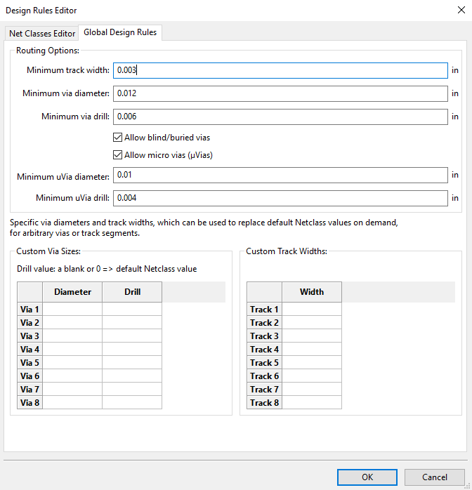
- Minimum Track Width: 3 mil (0.762 mm)
- Minimum Via Diameter: 12 mil (0.3048 mm)
- Minimum Mechanical Drill Size: 6 mil (0.1524 mm)
- Minimum Laser Drill Size [for micro-vias]: 4 mil (0.1016 mm)
- Minimum Micro-Via Diameter: 10 mil (0.254 mm)
These values reflect Bittele’s preferred global minimums, but in some cases we can allow for smaller sizes when necessary. If your project requires any parameters that violate those given above, please get in contact with one of our PCB Customer Service Experts for further advice.
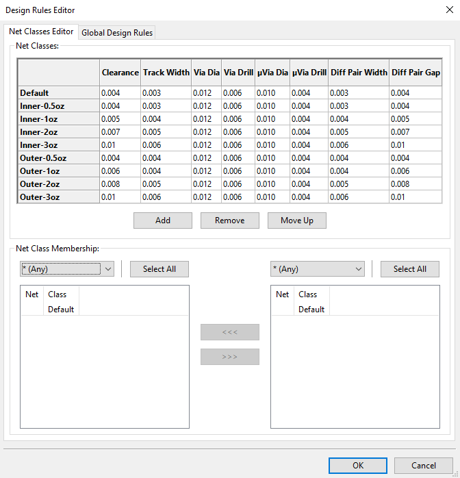
Please note that trace width and spacing requirements depend upon both the copper layer in question and the Copper Weight specified for that layer. The global minimum values given above apply to internal layers with 0.5 oz. copper weight. For Multilayer PCBs, we recommend that our clients set up individual design rules that can be applied to each layer depending upon its particular specifications. The image below shows our preferred trace width and clearance minimums for both internal and external layers, with copper weight values up to 3.0 oz.
On the topic of spacing, we would like to note that track spacing is not the only aspect to keep in mind. We also require at least a 4.0 mil solder mask gap between traces or SMT Assembly pads, and we observe a separate set of rules for PCB Part Spacing, as opposed to track spacing. Many CAD PCB layout software packages do not have options for these additional rules, but it is a good idea to check your software for additional design rule options. If these are not included as design rules in software, the PCB designer will have to keep these spacing requirements in mind, and carefully check the finished board before submission to Bittele in order to ensure that there will be no delay in the production process.
If you are having trouble setting up the design rules in your software, if you have a question about our capabilities, or to send in your PCB Design Files for an official quotation, please feel free to Contact Us any time! We can be reached via email at sales@7pcb.com, or toll-free at 1-888-812-1949.
Related Articles:
Please briefly describe the information you are seeking in the search bar below.