


 English
TURN-KEY PCB ASSEMBLY: BITTELE ELECTRONICS
PCB MANUFACTURING AND ASSEMBLY
Full Turn-Key PCB Manufacturer
You can quickly get quotes and order PCB fabrication and assembly using our online system. Take advantage of exclusive automatic discounts with our tool. Our BOM pricing tool ensures you receive the lowest price for your order.
START A TURN-KEY PCB ORDER
PLCC Component Packages
At Bittele Electronics, we pride ourselves on our ability to provide High Quality PCB Assembly for all electronic component package types. One of the lesser used IC package options is the PLCC, or Plastic Leaded Chip Carrier, which offers some distinct advantages particularly in the realm of Prototype PCB Assembly. This article will offer some basic information about the PLCC package type, followed by a brief discussion of the advantages of this package where the PCB Assembly Process is concerned. We hope that this will help clients of Bittele to make an informed decision regarding the best package options for the ICs in their PCB projects.
The PLCC package is a flexible option that allows for components to be either soldered directly onto the surface of the PCB, or mounted in a socket for easy removal. This flexibility allows for efficient prototyping without requiring a change in Component Packages when the project moves into higher volume production.
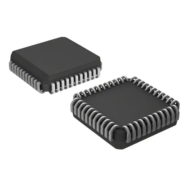
The flexibility of the PLCC package stems from its unique “J-lead” design, which describes the shape of the device’s contacts, as pictured above. This form factor results in smaller overall PCB footprints, compared to QFP packages, while avoiding the need for X-Ray Inspection that would be required for QFN packages. Perhaps most importantly, the PLCC package can fit easily into an IC socket, allowing for easy off-board programming and firmware updates, a particularly valuable benefit when it comes to recursive testing procedures for prototypes. PLCC packages are available in a variety of lead counts, from 20 to 84, and are also common for 2-pin LED components.
In addition to its design benefits, the PLCC package also boasts many advantages during PCB Assembly. The option to avoid the need for X-Ray Inspection, as mentioned above, will allow clients to reduce the cost on their Turnkey PCB quotations. We also generally advise our clients to opt for minimal changes between design revisions whenever possible, and the fact that the PLCC package can be used in a socket or mounted directly to the board makes it a great option for this recommendation. Though some revision will still be necessary once the board moves into production and the socket footprint is swapped out for the part footprint, Bittele’s DFM Checking procedure will be simplified by the fact that our production team is familiar with this exact part.
The main advantage of PLCC packages, both in terms of design and PCB production, comes into play for prototype designs where extensive IC Programming is required. Our general programming process at Bittele involves use of the project’s hex file to program the relevant ICs off-board, allowing for simpler PCB layouts that do not require built-in ICSP (In-Circuit Serial Programming) functionality. The PLCC package allows for the IC to be programmed concurrently with PCB Assembly, and mounted into its socket once assembly is complete.
If you are still not sure whether a PLCC package is right for your project, you can always reach out to one of Bittele’s PCB Customer Service Experts for advice. To send in your questions, or your PCB Design Files for an official quote, you can Contact Us any time at sales@7pcb.com, or toll-free at 1-888-812-1949.
Related Articles:
Please briefly describe the information you are seeking in the search bar below.