


 English
TURN-KEY PCB ASSEMBLY: BITTELE ELECTRONICS
PCB MANUFACTURING AND ASSEMBLY
Full Turn-Key PCB Manufacturer
You can quickly get quotes and order PCB fabrication and assembly using our online system. Take advantage of exclusive automatic discounts with our tool. Our BOM pricing tool ensures you receive the lowest price for your order.
START A TURN-KEY PCB ORDER
Circuit Board Footprints for SMT Power Electronics
As an industry-leading provider of High Quality PCB Assembly services since 2003, Bittele Electronics is well equipped to handle projects from any industry, including high power applications. We often receive questions from clients about PCB Layout for High Power, as well as requests for advice about Electronic Component Packages and footprints for such designs. This article is intended to quickly resolve these questions, and to give Bittele’s clients some insight into how their decisions in high power PCB Component Selection and footprint design can affect the PCB Assembly Process.
With the increasing necessity for smaller devices and HDI PCBs, electronic components have been trending smaller each year, and power electronics are no exception. Power consumption and heat dissipation are of course more difficult to manage as parts decrease in size; this was one critical advantage of Through-Hole PCB Assembly over SMT Assembly, and the reason why some engineers continue to use larger through-hole parts in their high power designs.
The trade-off between size and heat dissipation can be challenging at times, and has consequences in the PCB production process as well. Selecting a majority of SMT components reduces the need for Mixed SMT & THT Assembly. While Bittele can certainly provide mixed assembly, the assembly process is more efficient and less costly if a majority of your PCBs can be assembled using Reflow Soldering. A large number of through-hole components on a mixed assembly project will require additional time for Manual Assembly, or in some extreme cases a Wave Soldering cycle might be required in addition to the reflow cycle. Fortunately, surface mount components have been consistently evolving to meet the needs of high power projects. It is now possible to find a wide variety of surface mount parts designed specifically for higher power requirements, and Bittele Electronics has the expertise required to work with these components.
Common Footprints for Power Electronics
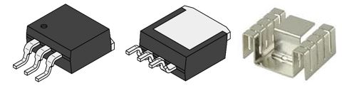
TO-263 (D2Pak) and TO-252 (DPak)
The most common package for through-hole MOSFET devices, as well as many voltage regulators, is the TO-220, which is commonly installed with an accompanying heat sink. The surface mount equivalents of this package are the TO-263 and the TO-252, also known as D2Pak and DPak. These packages incorporate large pads on their underside specifically for the purpose of heat dissipation, with separate heat sinks also available. DPak components are commonly rated for 50W power dissipation, with D2Pak parts commonly rated at 100W. These packages are no trouble for us at Bittele, and we recommend that clients select these packages as often as possible in place of the through-hole variant.
SOT-223 & SOT-323
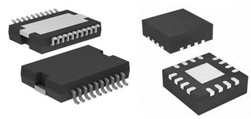
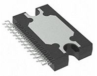
The SOT-223 and SOT-323 package types are not quite so robust as the DPak parts previously discussed, but they are viable in the 1W to 5W range, and are commonly used for BJT transistors. The SOT-223 includes a large tab that facilitates higher power dissipation, which normally makes it the better choice for higher-power applications. Again, these parts are well suited to Bittele’s standard reflow assembly process, so no special considerations must be made during production. Exposed Pad SOIC, TSSOP, QFP, and QFN Also commonly known as PowerQFN, PowerSOIC, etc., these packages are higher-power variants of familiar surface mount IC packaging. Power dissipation values for these parts vary largely depending upon the physical size of the IC, which in turn is normally dependent upon its number of pins, so clients are advised to check these part datasheets carefully. That being said, the large pad located in the center of the device can greatly increase dissipation when connected to a metal plane on the PCB.
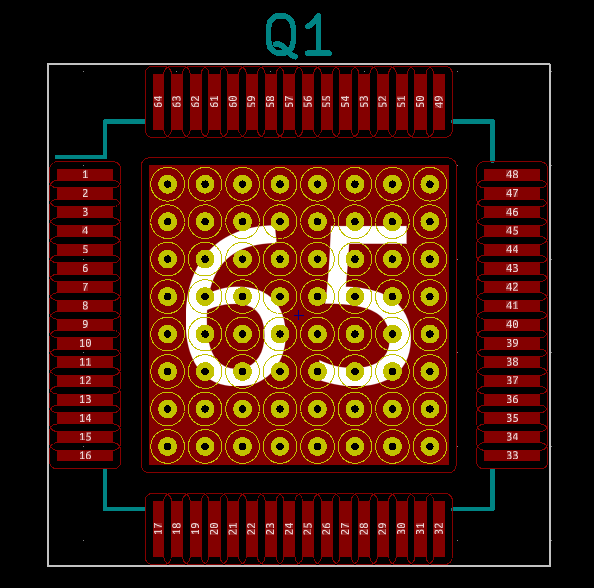
Connecting the exposed pads for these parts to ground planes requires vias, and datasheets will frequently suggest that an array of vias be used for maximum dissipation. Some of our clients have asked if this will incur additional charge for Via in Pad filling, but this special service is only necessary for smaller pads, where solder has a tendency to wick away and down the via. No additional cost or lead time will be incurred for vias in thermal relief pads.
Less Common Power Electronics Footprints
This article has explicitly covered only the most common SMT footprints for power electronics, and many more exist. Bittele’s production team is extremely well-versed in all of these package types, and our Standard Price PCB Options cover the vast majority of package types. If you are unsure about the footprint in your design, it never hurts to get in touch with one of our PCB Customer Service Experts.
To reach out with your questions, or to send along your PCB Design Files for an official quotation, please feel free to Contact Us any time! You can reach us over email at sales@7pcb.com, or call us toll-free at 1-888-812-1949.
Bittele is a full-service provider of low-cost Canada-Based PCB Assembly solutions. In business since 2003, we have established ourselves as a leader in the PCB production industry, and we offer a variety of tailored solutions to meet your specific needs.
Related Articles:
Please briefly describe the information you are seeking in the search bar below.