


 English
TURN-KEY PCB ASSEMBLY: BITTELE ELECTRONICS
PCB MANUFACTURING AND ASSEMBLY
Full Turn-Key PCB Manufacturer
You can quickly get quotes and order PCB fabrication and assembly using our online system. Take advantage of exclusive automatic discounts with our tool. Our BOM pricing tool ensures you receive the lowest price for your order.
START A TURN-KEY PCB ORDER
Overview of Embedded Components
Embedding Discrete SMT Components into Multilayer PCBs
In recent years, there has been a growing trend of embedding SMT resistors and capacitors into the internal layers of PCBs. This approach is typically used when only a small number of components are required, or components with non-standard resistance or capacitance values. It is also applicable when PCB thickness is not a limiting factor specifically, when the dielectric layer thickness exceeds the height of the chip component itself.
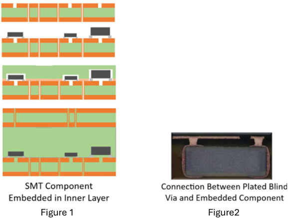
A conceptual illustration of embedding chip components into PCB inner layers is shown in Figure 1. There are two primary methods for embedding chip components into internal layers of a PCB:
- Adhesive Fixed with Laser Via Interconnection
The chip component is fixed onto the inner layer using adhesive. After lamination, laser drilled microvias are created at both terminals of the component to establish electrical interconnection. See Figure2. - Direct Soldering onto Inner Pads
The chip component is soldered directly onto the inner layer pads before being laminated into the PCB stackup.
Key Manufacturing Challenges
Embedding SMT components introduces several processing challenges:
- Precise Component Placement
High accuracy is required during placement to prevent misalignment during lamination. Components must remain fixed and must not shift due to adhesive flow during the lamination process. - Lamination Material Process Control
Selection of proper lamination materials is critical. Typically, a thin FR-4 prepreg is used as a reinforcement layer. The cutout dimensions and flow characteristics of the adhesive are crucial. Internal surface treatment must avoid damaging the embedded components, and the lamination pressure must be controlled to prevent cracking of the components. - Layer Registration and Dimensional Stability
Accurate registration between internal layers and compensation for material expansion/contraction during pressed lamination are essential for successful integration. - Laser Drilling Precision
When using laser-drilled blind vias, the laser energy must be precisely controlled to stop at the component electrode surface without damaging it. This process also requires high-precision alignment to ensure proper via-to-pad connection.
To get started on your PCB design with Bittele, or for general PCB questions you can contact us anytime! To receive your official quote, please send in your board design files to sales@7pcb.com. We can also be reached at 1-416-800-7540.
Related Articles:
Please briefly describe the information you are seeking in the search bar below.