


 English
TURN-KEY PCB ASSEMBLY: BITTELE ELECTRONICS
PCB MANUFACTURING AND ASSEMBLY
Full Turn-Key PCB Manufacturer
You can quickly get quotes and order PCB fabrication and assembly using our online system. Take advantage of exclusive automatic discounts with our tool. Our BOM pricing tool ensures you receive the lowest price for your order.
START A TURN-KEY PCB ORDER
How to Mitigate EMC and EMI in PCB Design?
In electronic engineering, designing a PCB (Printed Circuit Board) layout is a crucial task that demands careful attention to detail, particularly in preventing Electromagnetic Interference (EMI) and ensuring Electromagnetic Compatibility (EMC). EMI can disrupt circuit performance, while EMC ensures that a system operates effectively in its electromagnetic environment without causing harmful interference. Identifying potential EMI/EMC issues early in the design phase is essential to minimize costly revisions and enhance the reliability of electronic devices.
To mitigate EMC/EMI issues in PCB design, consider the following strategies:
1. Proper Grounding
Grounding provides a common reference point for all signals in a circuit, which is essential for maintaining signal integrity and reducing noise. Proper grounding minimizes the loop area for return currents, thereby reducing EMI.
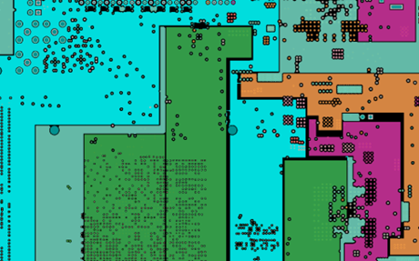
Improper grounding can result in increased signal noise, crosstalk between circuits, and overall system instability. This often occurs when designers fail to implement a continuous ground plane or introduce splits in it. To mitigate this issue, use a solid ground plane to ensure an unbroken, low-impedance path for return currents. Avoid splitting the ground plane, as these forces return currents to take longer paths, increasing the loop area and EMI.
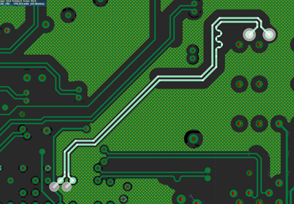
2. Trace Layout
The layout of PCB traces significantly impacts EMI, as traces can act as antennas, either emitting or receiving electromagnetic interference. Poorly routed traces such as those forming large loops or running parallel to noisy signals can amplify EMI issues.
To minimize EMI, keep traces short and direct to reduce their antenna effect. Use 45-degree angles instead of 90-degree bends to avoid impedance discontinuities. And maintain proper trace spacing to minimize crosstalk between signal lines.

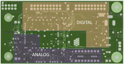
3. Component Placement
Component placement plays a crucial role in the PCB’s performance and its susceptibility to EMI. Sensitive components placed too close to noisy ones can experience interference. Designers often overlook the importance of strategic component placement, which can lead to noise coupling and signal integrity issues.
To optimize board performance, group components by its function by placing analog and digital components in separate areas to reduce interference. And keep high-frequency components away from sensitive analog circuits to prevent unwanted noise coupling.
4. Shielding
Shielding involves enclosing sensitive PCB components with conductive materials to block EMI. Inadequate shielding can allow electromagnetic radiation to escape or external interference to affect the circuit.
To improve shielding, use metal shields around high-frequency components to contain EMI. Implement ground plane shielding by placing dedicated ground layers beneath signal traces to absorb and dissipate electromagnetic energy. And design conductive enclosures for sensitive components to further prevent EMI.
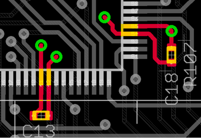
5. Decoupling Capacitors
Decoupling capacitors filter noise from the power supply, ensuring a stable voltage for ICs. Improper placement or insufficient use of decoupling capacitors can lead to power supply noise, degrading circuit performance.
To enhance stability, place capacitors as close as possible to IC power pins to minimize inductance. Also, it is recommended to use multiple capacitors with different values to filter a broad range of frequencies.
6. Controlled Impedance
Controlled impedance ensures that PCB trace impedance matches the connected components, preventing signal reflections and preserving signal integrity. Mismatched impedance can lead to reflections, increasing EMI and causing signal degradation.
To achieve proper impedance control, design traces with specific widths, spacing, and dielectric materials to maintain the desired impedance. Use differential pairs for high-speed signals to reduce EMI and improve signal integrity and ensure impedance consistency throughout the trace length to prevent signal distortions.
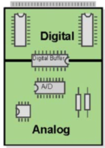
7. Segregating Analog and Digital Grounds
Separating analog and digital grounds prevents digital noise from contaminating sensitive analog signals. Merging these grounds improperly can lead to noise coupling and signal integrity issues.
To prevent interference, use separate ground planes for analog and digital sections of the PCB and connect the analog and digital grounds at a single point to prevent ground loops.
By following these detailed guidelines, designers can effectively mitigate EMC/EMI issues in PCB design, ensuring reliable and high-performance electronic systems.
For more information about our capabilities or to send us your PCB Design Files for an official quotation, please feel free to Contact Us any time! We can be reached via email at sales@7pcb.com or call at 1-416-800-7540.
Related Articles:
Please briefly describe the information you are seeking in the search bar below.