


 English
TURN-KEY PCB ASSEMBLY: BITTELE ELECTRONICS
PCB MANUFACTURING AND ASSEMBLY
Full Turn-Key PCB Manufacturer
You can quickly get quotes and order PCB fabrication and assembly using our online system. Take advantage of exclusive automatic discounts with our tool. Our BOM pricing tool ensures you receive the lowest price for your order.
START A TURN-KEY PCB ORDER
Eliminating Ambiguity in Your PCB Designs
At Bittele Electronics, our specialty is efficient and high-quality Complete PCB Assembly, and we do our utmost to work with our clients every step of the way to make this process better. We pride ourselves on our straightforward PCB Assembly Process, where we handle every step of the process, including DFM Checking, Parts Procurement, PCB Fabrication, Electrical Testing, PCB Assembly, and Final Inspection / Testing. Bittele provides high-quality PCB Assembly in Canada, and we have been industry leaders in PCB service since 2003. Through those years of experience, we have tailored our processes to be as simple and efficient as possible for you, our valued client. In turn, there are a few strategies that you can employ as a PCB designer to make the process even more efficient and to ensure a perfect build the first time.
When you choose our Turnkey PCB Assembly service, all you need to do is send along your PCB Design Files, and we send back a tested and fully functional board. As such, our process operates at its maximum efficiency when your design is as clear and unambiguous as possible. Bittele’s Quality Management team is extremely adept at catching these types of errors before production begins, but inconsistent or ambiguous data in design files will prompt additional questions, and potentially increase the overall project lead time. Most commonly, these types of issues arise when information in one document disagrees with information in another, so a thorough check that all of your files reflect the most recent design revision can pre-empt many questions during production.
Aside from general consistency between design files, there are a few more specific strategies for eliminating ambiguity in each of the four main types of design files that Bittele requires:
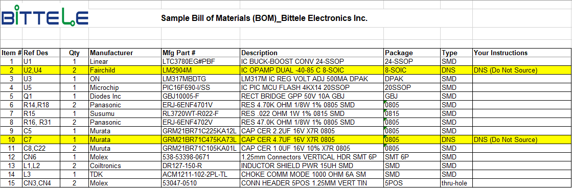
Bill of Materials (BOM) Clarity
Most CAD programs for PCB Layout offer automatic generation for your Bill of Materials (BOM) based on Reference Designators, footprints, and component values specified during the schematic design phase. These options can be used to save on time and minimize common errors such as mismatches between the quantity and the number of reference designators. That being said, a manual review of the software-generated BOM is still essential to ensure its overall clarity.
Some of the most common BOM issues that Bittele has noticed in the past are listed below:
- Incomplete, ambiguous, or missing Part Numbers
- Quantity to reference designator mismatches
- Part number to description mismatches
At the very least, your BOM should include complete information on Quantity, Reference Designators, and Part Number on each line. To further protect against potential delays or confusion, it is helpful to include information about Manufacturer, Description, and Additional Instructions where applicable.
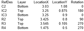
Centroid Clarity
Clarity in the Centroid File – also known as XY-Coordinate or Pick & Place file – is extremely important, since this data will be directly used to program Bittele’s Pick and Place machines for Automated Part Placement. Centroid data is Generated Directly by the CAD Software used for PCB layout, but this does not make it immune to inaccuracy or ambiguity. The following issues are the most common for Centroid data:
- Disagreement with the BOM, usually due to project updates not reflected in one document
- Missing parts, usually due to errors in the CAD software
- Inaccurate coordinates, usually due to a Gerber file update without generating a new Centroid
A sample Centroid file is shown below:
Gerber File Clarity
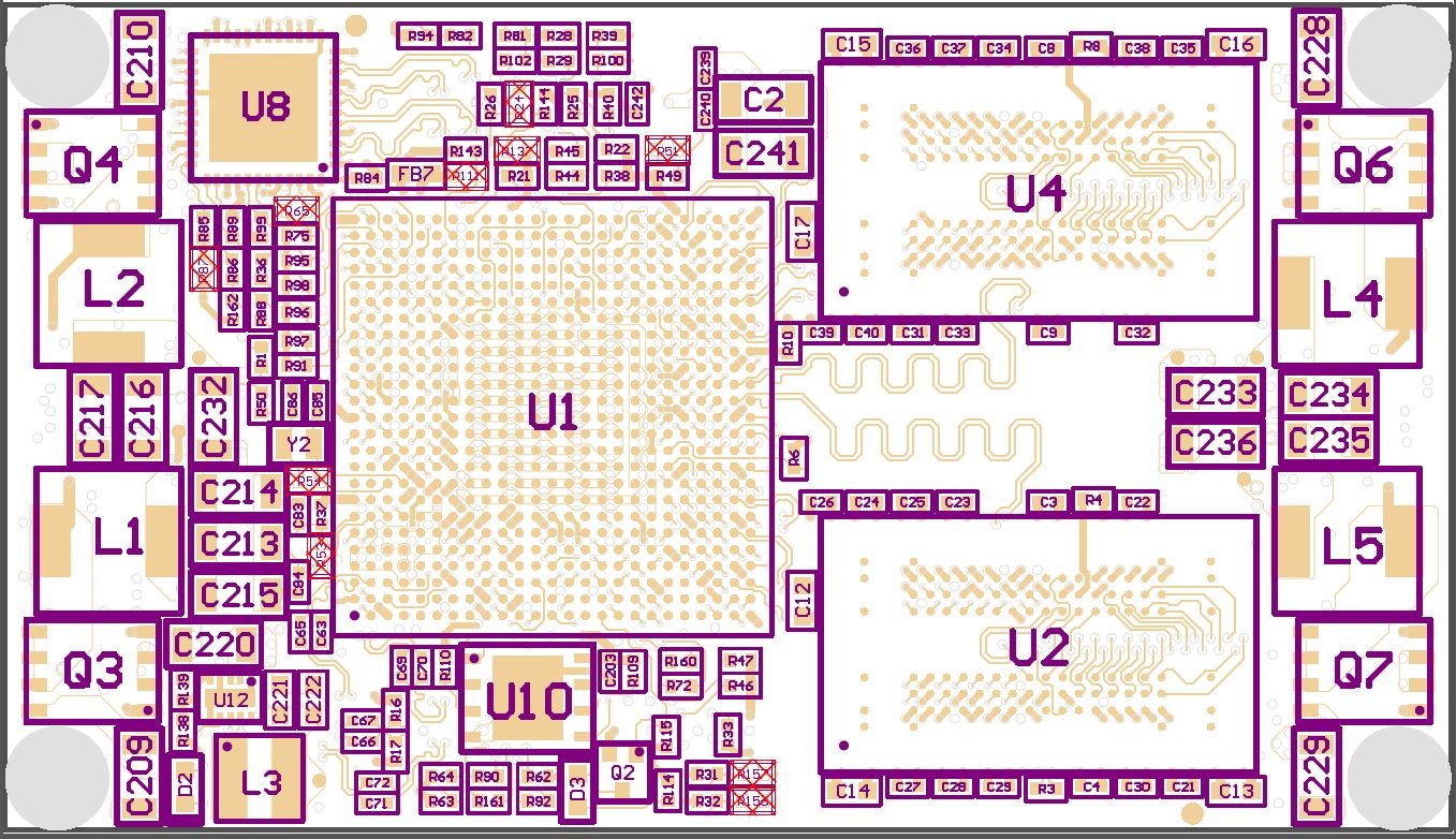
The first thing to note about Gerber Files and their role in PCB Assembly is the Silkscreen Layer. This layer shows reference designators for specific components beside their associated Land Patterns. During Bittele’s initial DFM / DFA check sequence, these reference designators are compared with those in the BOM and Centroid files to ensure that any errors in one file are caught early and brought to the client’s attention. The silkscreen layer also contains markings for the Orientation of Polarized Components, which can help to avoid questions and potential issues during assembly.
Some High-Density Interconnect (HDI) boards do not have enough room between components for a silkscreen layer, and some clients simply do not want to include silkscreen markings on the finished board for aesthetic reasons. In this case, Bittele will require assembly drawings or mechanical Gerber layers to act as a substitute for the silkscreen layers.
Issues around Gerber file clarity in PCB Assembly are often a result of design revisions that are not reflected across all files, causing a discrepancy between the Gerbers and the BOM, Centroid, or Assembly Drawing. Notes are sometimes copied from a previous design to save time, but design differences are sometimes overlooked in this case; it is recommended to use an empty notes template and fill it for each project individually to minimize these sorts of errors.
Assembly Drawing Clarity
Assembly drawings are a supplementary file, used to offer additional clarity on the required PCB assembly, and to describe in detail any special requirements for the project in question. Most PCB Layout software suites include an option for generating assembly drawings, which will generally output to PDF both a top-down and a bottom-up view of the board, as below:
A basic assembly drawing, such as the one shown above, can help to clarify specific placements and DNI (Do Not Install) parts, and is sometimes necessary to provide more information about special requirements. Processes such as Functional Testing, as well as specifications for temperature tolerances, flux and solder types, or manual assembly parts, should be included in the assembly drawing. These types of specifications can be added on a separate page of the PDF document or simply included in the margins of the drawings themselves.
Bittele Electronics recommends including at least a basic assembly drawing with any PCB Assembly project submission. As a general rule: the more information that is included on the drawing, the fewer the number of questions asked during assembly.
If you still find yourself with any questions of your own regarding clarity and ambiguity in your PCB designs, please feel free to Contact Us any time! We can be reached via email at sales@7pcb.com, or toll-free at 1-888-812-1949.
Related Articles:
Please briefly describe the information you are seeking in the search bar below.