


 English
TURN-KEY PCB ASSEMBLY: BITTELE ELECTRONICS
PCB MANUFACTURING AND ASSEMBLY
Full Turn-Key PCB Manufacturer
You can quickly get quotes and order PCB fabrication and assembly using our online system. Take advantage of exclusive automatic discounts with our tool. Our BOM pricing tool ensures you receive the lowest price for your order.
START A TURN-KEY PCB ORDER
Controlling Warpage in High-Layer PCBs
During PCB fabrication and assembly, it’s common to encounter boards with excessive warpage (exceeding the IPC standard of 0.75%). Such warpage during the SMT assembly process can lead to misalignment, preventing components from being properly inserted into through-holes or aligned with surface-mount pads and poor soldering quality. This often results in soldering defects such as cold joints or open circuits.
Understanding the root causes of warpage during fabrication and how to mitigate them during the design phase is critical to maintaining PCB quality and soldering reliability.
Common Causes of Warpage in High-Layer PCBs
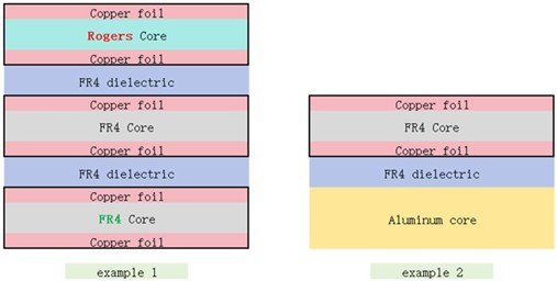
1. Material Asymmetry
To meet performance or cost requirements, designers may choose to use hybrid material constructions in a single PCB, such as combining high-frequency materials with standard FR4 (see Example 1), or FR4 with metal core reinforcements (see Example 2).
When different materials are stacked asymmetrically across the board, imbalance or inconsistent coefficients of thermal expansion (CTE) can result in significant warpage after lamination and reflow process. This occurs because different materials expand and contract at different rates during thermal processing.
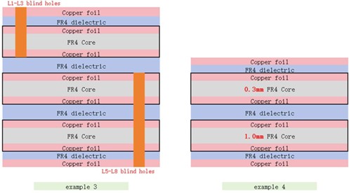
2. Structural Asymmetry
Designs with mechanically drilled blind/buried vias or asymmetric material stackup can create imbalance. For example, in an 8-layer board with L1–L3 and L4–L8 blind vias (see Example 3) may be laminated in two separate sub-assemblies before final lamination process. This results in bonding two structurally different sub-assemblies, making warpage control difficult.
Similarly, using core materials of different thickness in asymmetrical stackup to meet impedance or other requirements (see Example 4) can also cause warpage, even if the material type is the same, due to unequal rate of thermal expansion resulting in deformation.
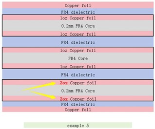
3. Copper Weight Imbalance
To support higher current requirement or improve thermal performance, designers may use thicker copper on certain layers in stackup (see Example 5). If this is done asymmetrically, the imbalance in copper thickness leads to uneven heat absorption and stress during lamination, resulting in board warpage.
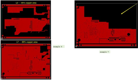
4. Pattern Design Imbalance
Significant differences in copper pour or copper density in board design across symmetrical layers can also lead to warpage. For instance, in 8-layer board (see Example 6), such as 30% or greater difference in copper area between L2 and L7 can also cause warpage.
Additionally, if one side of a layer has large copper-free “empty” areas (see Example 7) while the opposite side is fully copper-filled, the imbalance in thermal expansion between copper and dielectric material (FR4) can cause localized or overall deformation.
Conclusion and Design Recommendations
While PCB manufacturers can use mitigation techniques such as pre-baking, flattening, and controlled cooling, if the root causes above exist in the design, warpage is difficult to fully eliminate and can increase assembly complexity or cause long-term reliability issues especially for fine-pitch or high-reliability components.
To minimize warpage in high-layer PCBs and ensure high soldering quality especially for precision components, designers should avoid asymmetric material stacks (e.g., hybrid builds or uneven reinforcement). Maintain stackup symmetry for blind/buried vias and core thickness. Balance copper weights and copper density across layers. Follow IPC-2226 guidelines for high-density interconnect (HDI) stackup design. And collaborate with your PCB fabricator early to verify stack feasibility.
For more information about our capabilities or to send us your PCB Design Files for an official quotation, please feel free to Contact Us any time! We can be reached via email at sales@7pcb.com or call at 1-416-800-7540.
Related Articles:
Please briefly describe the information you are seeking in the search bar below.