


 English
TURN-KEY PCB ASSEMBLY: BITTELE ELECTRONICS
PCB MANUFACTURING AND ASSEMBLY
Full Turn-Key PCB Manufacturer
You can quickly get quotes and order PCB fabrication and assembly using our online system. Take advantage of exclusive automatic discounts with our tool. Our BOM pricing tool ensures you receive the lowest price for your order.
START A TURN-KEY PCB ORDER
Raw Material Choices for PCBs
This article provides recommendations for choosing materials to manufacture multilayer PCBs that achieve two critical requirements: limit manufacturing problems (e.g., bowing or twisting, as well as mis-registering; and meeting performance standards. A successful PCB production begins with proper material selection. For a low number of board layers, your PCB manufacturers default materials are usually your best choice as they are reliable and cost effective. However, when designs have special requirements or incorporate a high number of layers, then it is worth a designer’s effort to become more familiar with the available material options, in order to make the best decisions for their product.
The most important material for PCB manufacturing is raw laminate. It also represents the largest cost of all other materials needed to produce a multilayer PCB. Raw laminate has a critical impact for the prices and the delivery time of PCBs. Due to the amount of material needed for PCB fabrication, it is essential to optimize the size of your designs; even a small difference in size can result in a significant difference in cost. Different materials incur different costs and possess different characteristics, but higher quality laminates are typically also more expensive. The following are some of the main characteristics to take note of when comparing properties of different laminates:
Tg = Glass Transition Temperature – Temperature at which a critical change of physical properties will occur. In the case of laminates, it transitions from a hard, glassy material into a soft, rubbery material
Td = Decomposition Temperature - Temperature at which the laminate chemically decomposes
Dk = Dielectric Constant (also referred to as εr in electromagnetics) – Indicates the relative permittivity of an insulator material, which refers to its ability to store electrical energy in an electric field. For insulating purposes, a material with lower dielectric constant is better and in RF applications a higher dielectric constant may be desirable
Df = Dissipation Factor – Indicates the efficiency of an insulating material by showing the rate of energy loss for a certain mode of oscillation, such as mechanical, electrical, or electromechanical oscillation
Our fabrication facilities are located in China, so it is advisable to choose high-quality local laminates in order to minimize shipping cost and lead time. The Shengyi S1000-H (Tg 150) laminate is generally our default choice for a high-performance, mid-Tg laminate. Shengyi S1000-H is comparable to Isola FR406 (Tg 150), a standard North American laminate option. As outlined in Table 2 below, FR406 does slightly outmatch Shengyi S1000H in terms of Dielectric Constant and Dissipation Factor, but some clients may be willing to compromise on these factors for a lower cost and/or a faster lead time.
Table 1: Comparison of PCB Materials
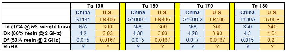
Shengyi S1141 (TG 130) is a good alternative to lower the cost of your project, at the sacrifice of some quality. In cases where higher quality is needed, we recommend Shengyi S1000-2M (TG 170) which is the closest in quality to Isola FR406 (Tg 170). Where quality is the highest priority, we would recommend utilizing ITEQ IT180A (TG 180) which is also RoHS compliant. ITEQ IT180A (TG 180) is comparable in quality and to Isola 370HR (TG 180). We at Bittele would suggest using Shengyi S1000H (Tg 130) for typical projects. We would recommend using one of the higher quality laminate materials if any of these three conditions occur: if the PCB Design has 8 or more layers, if Copper Board is heavy with a copper weight heavier than 3oz, or if PCB Board is thin with a board thickness of less than 0.5mm.
The next element to consider is the dielectric thickness, which must be specified for impedance requirements. Multilayer materials range from 0.125mm to 1mm in thickness. Thin laminates (i.e. 0.1mm or less) are necessary for some low-power applications as well as the continued densification of multilayer circuit PCBs. You may specify your own layer stackup or use one of our recommended options outlined in this document: Multi layer stack up
Table 2 lists the core material thickness with copper weight for normal FR4 Material
- 1/1 = 1 oz. copper per square foot on BOTH sides of the sheet
- 1/0 = 1 oz. copper per square foot, coated on only 1 ONE side of the sheet
- H/H = 0.5 oz. copper per square foot, coated on BOTH sides of the sheet
- 0/0 = UNCLAD (NO Copper).
Table 2: Core material thicknesses at available copper weights
| Thickness including copper (mm.) | Copper Weight (oz.) |
|---|---|
| 0.145 mm. | H/H oz. |
| 0.17 mm. | 1/1 oz. |
| 0.185 mm. | H/H oz. |
| 0.2 mm. | 1/1 oz. or H/H oz. |
| 0.25 mm. | 1/1 oz. or H/H oz. |
| 0.3 mm. | 1/1 oz. or H/H oz. |
| 0.4 mm. | 1/1 oz. or H/H oz. |
| 0.5 mm. | 1/1 oz. or H/H oz. |
| 0.6 mm. | 1/1 oz. or H/H oz. |
| 0.7 mm. | 1/1 oz. or H/H oz. |
| 0.8 mm. | 1/1 oz. or H/H oz. |
| 0.9 mm. | 1/1 oz. or H/H oz. |
| 1.0 mm. | 1/1 oz. or H/H oz. |
| 1.1 mm. | 1/1 oz. or H/H oz. |
| 1.2 mm. | 1/1 oz. or H/H oz. |
| 1.5 mm. | 1/1 oz. or H/H oz. |
| 1.6 mm. | 1/1 oz. or H/H oz. |
| 2.2 mm. | 1/1 oz. |
| 2.4 mm. | 1/1 oz. |
| 2.5 mm. | 1/1 oz. |
| 3.0 mm. | 1/1 oz. |
Prepreg is a bonding material used in the fabrication of multi-layer PCB boards which, after curing has the same properties as the core /base layer materials. Prepregs have various glass styles 106, 1080, 3313, 2116 and 7628 used by board fabricators. Board fabricators use a variety of prepreg glass styles. These styles include 106, 1080, 3313, 2116 and 7628. Limitations may apply to the number and types of prepreg, so it is best to contact a Bittele representative for further details.
Table 3: Prepeg material choices
| Prepreg /Glass Styles | Pressed Thickness (mm) | Prepreg Resin content |
|---|---|---|
| 106 | 0.05 mm. | Approx. 73% |
| 1080 | 0.075 mm. | Approx. 65% |
| 3313 | 0.09 mm. | Approx. 57% |
| 2116 | 0.115 mm. | Approx. 55% |
| 7628 | 0.185 mm. | Approx. 46% |
| 7628H | 0.195 mm. | Approx. 51% |
Lastly, the thickness of copper layers should be specified. This specification is usually decided based on the amount of current that is expected to pass through the traces of a board. Use our Trace Width Calculator to determine standard trace widths for a given copper thickness. Thicker traces can safely handle more current than thinner traces of the same width. You may also wish to specify thicker copper layers for a more robust board if you expect the board to be operating in harsh conditions.
Copper clad FR-4 laminate materials are measured using ounce(oz.) weight per square foot. The following are available sizes and their equivalent layer thickness
- 0.25 oz. = 0.00035” (8.75μm)
- 0.5 oz. = 0.0007” (17.5 μm)
- 0.75 oz. = 0.00105” (26.25μm)
- 1.0 oz. = 0.0014” (35 μm)
- 2.0 oz. = 0.0028” (70 μm)
- 3.0 oz. = 0.0042” (105 μm)
- 4.0 oz. or more = 0.0056” (140 μm) or more
Bittele Electronics is capable of fabricating multi-layer PCB boards with a maximum copper weight of 10 oz. Copper weight of 4 oz. or higher will require an additional estimate, and may also affect lead times.
Related Articles:
Please briefly describe the information you are seeking in the search bar below.