TURN-KEY PCB ASSEMBLY: BITTELE ELECTRONICS
PCB MANUFACTURING AND ASSEMBLY
Full Turn-Key PCB Manufacturer
You can quickly get quotes and order PCB fabrication and assembly using our online system. Take advantage of exclusive automatic discounts with our tool. Our BOM pricing tool ensures you receive the lowest price for your order.
START A TURN-KEY PCB ORDER
PCB Transmission Line Considerations
At Bittele Electronics we take every aspect of your project seriously and try to accommodate all requests and project specifications. One such specification is Controlled Impedance, to achieve the required Impedance values Bittele’s Engineering Team may need to change certain specifications such as the thickness of the dielectric or the height and width of the specific trace.
One of the factors that need to be considered for impedance control are the transmission line effects. Ignoring the transmission line effects can have major impacts on the quality of the signal being passed.
A PCB Transmission line is made up of two conductors, one that carries a signal and the other is the return path which is usually the ground. When a PCB Transmission line has the same impedance and line geometry at every point then it can be considered a controlled impedance line. A trace and its return path are considered to be a PCB Transmission line when the time it takes for the signal to move from the source to the destination cannot be ignored.
There are three basic types of PCB Transmission lines:
- Microstrip
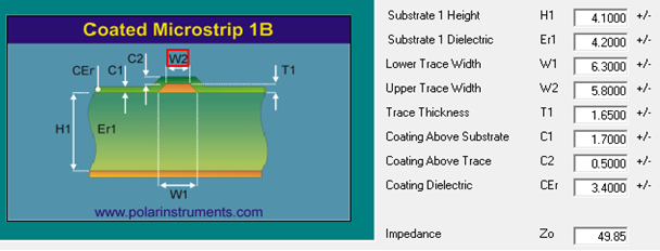
The microstrip transmission line has its signal trace routed on one of the external layers of the board with a dielectric material separating it from its reference/ground plane. This can be seen in the image below along with the variables that affect the impedance of the line:
- Stripline
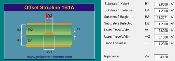
The stripline transmission line has an internal signal trace that is surrounded by dielectric material. The dielectric material is between two reference/ground planes. This can be seen in the image below along with the variables that affect the impedance of the line:
- Coplanar
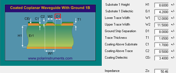
The coplanar transmission line is an external signal trace that has its reference/ground traces on both sides of it. Thus there are three conductors in total, the separation between the signal trace and the reference/ground traces is the same along the entire length of the line. This can be seen in the image below along with the variables that affect the impedance of the line:
Related Articles:
Please briefly describe the information you are seeking in the search bar below.






 English