


 English
TURN-KEY PCB ASSEMBLY: BITTELE ELECTRONICS
PCB MANUFACTURING AND ASSEMBLY
Full Turn-Key PCB Manufacturer
You can quickly get quotes and order PCB fabrication and assembly using our online system. Take advantage of exclusive automatic discounts with our tool. Our BOM pricing tool ensures you receive the lowest price for your order.
START A TURN-KEY PCB ORDER
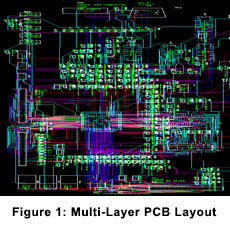
PCB Layout and Assembly
The first step in any design is creating the circuit diagram. Once the circuit diagram is finalized, PCB design and layout phase starts. Any circuit is designed on paper or in circuit design software to be easily understandable but the PCB design doesn’t have to fulfill this requirement. Although the connections on a circuit diagram and PCB design are kept the same; a PCB layout is more functional and designed to save space and follow different guidelines.
There are many different types of software that help in PCB design and layout. Softwares like ADS or ARES can automatically create a PCB layout once you give them the circuit diagram but for more complicated designs, the layout has to be done manually to ensure optimization. Connections can be routed manually or depending upon the PCB layout software, they can be done manually.
Types of PCB layout
There are many different types of PCB layout. The PCB layout for high frequency RF PCB is different than conventional style PCB layout for digital applications. Therefore, broadly categorizing, we have digital PCB layouts, RF PCB layouts, antenna layouts and power supply layouts. All the different types of layouts have their own guidelines which need to be followed for example in RF, we have to keep the reflections in transmission line to a minimum and ensure that there are no transmission lines close to each other which can affect the signal. On the other hand in a PCB layout for any digital application, we keep the copper tracks as close as possible to save space and minimize cost. Similarly for antenna layouts, we have to maximize the gain and for any PCB layout of a power supply, heat dissipation is the main concern.
PCB assembly
After the layout and design and layout are done, PCB assembly process starts. A PCB is created using any chosen material, most commonly, FR4. The electronic components are fit onto the PCB using a variety of assembly processes such as surface mount technique or a through-hole construction. The components used should also be compatible with the assembly process used.
Choice of PCB assembly
The choice of PCB assembly depends upon the complexity of the PCB design. Surface mount assembly technique is increasingly gaining popularity because it helps in miniaturizing any PCB. For a high frequency RF PCB, surface mount assembly reduces the noise and reflections and for any PCB where these restrictions don’t apply, we choose a PCB assembly which minimizes cost.
Cost comparison of layout and assembly
Layout costs completely depend upon the complexity of PCB design. For a multi-layered high-speed design the cost of layout is very high. This cost includes the tools which are required for this type of layout and the cost of hiring a capable designer. The assembly cost depends upon the type and quality of the assembly process used. The cost of layout and design are dependent upon each other as well. Also, if the layout is poor, the assembly costs might be greater and a better PCB layout can reduce the assembly and production costs.
Related Articles:
Please briefly describe the information you are seeking in the search bar below.