


 English
TURN-KEY PCB ASSEMBLY: BITTELE ELECTRONICS
PCB MANUFACTURING AND ASSEMBLY
Full Turn-Key PCB Manufacturer
You can quickly get quotes and order PCB fabrication and assembly using our online system. Take advantage of exclusive automatic discounts with our tool. Our BOM pricing tool ensures you receive the lowest price for your order.
START A TURN-KEY PCB ORDER
Manufacturing Considerations for Via in Pad PCB Designs
There are many reasons a via might need to be placed on top of the pad for a surface-mount component. The purpose of this article is to help Bittele’s clients to recognize the circumstances in which these types of vias necessitate extra work during production, requiring extra lead time and cost.
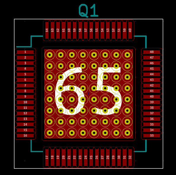
It is common for larger QFP and QFN packages to incorporate a large central pad for thermal relief purposes. These large thermal relief pads often require multiple vias to connect the pad to the ground plane of the PCB. These types of vias in pads can be built reliably with no additional cost or lead time.
The other reason for vias in pads is for ease of routing. As PCB size requirements become smaller and smaller, while pin counts for complex devices continue to grow, PCB designers and manufacturers are finding new and innovative ways to route the connections on their boards. Many of today’s HDI (High Density Interconnect) designs use Blind and Buried Vias, also known as micro-vias, to conserve space while making connections between layers.
For parts with a very high density of pins/pads, even micro-vias might not be sufficient, and the Via on Pad technique is often used. This can help immensely to escape traces from very fine pitch BGAs, or to connect bypass capacitors as close to a part as possible, but it does require some additional attention during the PCB production process.
The vias in these smaller surface mount pads tend to wick solder away from the pad itself, which can disrupt the PCB Assembly process and result in a non-functional pad. To avoid this issue, Bittele’s production team will fill the via with a non-conductive epoxy prior to assembly. This process requires both time and material, so clients should expect to see additional lead time and cost on their PCB quotations for designs incorporating these sorts of vias on pads.
If only a small number of vias need to be filled, then Bittele will often waive this cost for clients. The flowchart below shows the conditions under which vias must be filled, requiring additional cost and lead time. For more information about Bittele’s Via in Pad policies, feel free to Contact Us by email at sales@7pcb.com or toll-free at 1-888-812-1949.
Related Articles:
Please briefly describe the information you are seeking in the search bar below.