


 English
TURN-KEY PCB ASSEMBLY: BITTELE ELECTRONICS
PCB MANUFACTURING AND ASSEMBLY
Full Turn-Key PCB Manufacturer
You can quickly get quotes and order PCB fabrication and assembly using our online system. Take advantage of exclusive automatic discounts with our tool. Our BOM pricing tool ensures you receive the lowest price for your order.
START A TURN-KEY PCB ORDER
IC Packaging
Integrated Circuits, commonly known as ICs, form the backbone of the electronics industry today. It is rare to see a modern PCB project that does not incorporate at least one IC as a crucial part of its design. ICs are manufactured on silicon wafers through a process called photolithography, but the raw silicon dies are extremely fragile, and cannot often connect directly to external circuitry. To use the prepared ICs in PCB Assembly, a process known as encapsulation introduces a plastic or ceramic housing for the silicon die of the IC. The encapsulation provides physical durability, creates a hermetic seal to block environmental moisture, and improves the heat dissipation of the device. Perhaps most importantly of all, the encapsulation provides a means for electrical connection between the die and external electronics, such as a PCB.
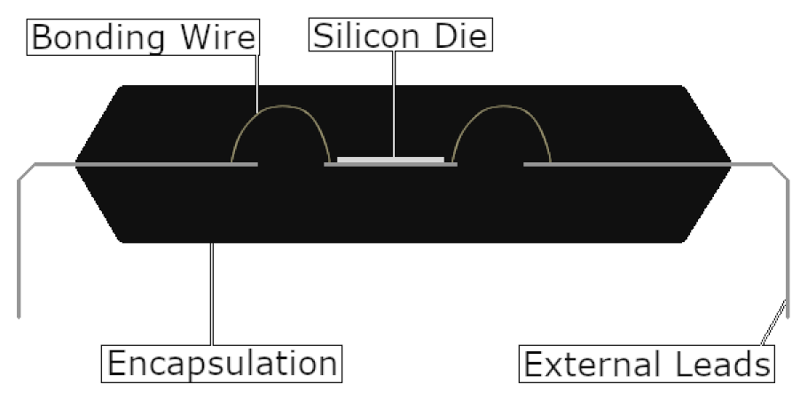
The image above shows a cross-section of an encapsulated die in a Dual-Inline Package (DIP), which is among the most rudimentary IC packages, not often used in modern PCBs. When you choose an IC for your PCB project, you will likely decide between a variety of Common Surface Mount Devices, including BGA, QFN, QFP, PLCC, and POP components. Many complex components, such as microprocessors and microcontrollers, will come in a variety of different packaging options. For detailed information regarding the individual properties of the aforementioned package types, please see the articles at the given links. The important thing to note here is that the type of packaging you select does not impact the electrical functionality of the IC itself.
From a PCB layout designer’s point of view, the most important properties in selecting an appropriate IC package are its physical size and the associated ease in PCB Assembly. For example, BGA and QFN packages offer a small profile, which relaxes the spatial constraints of the PCB layout design compared to larger QFP components. Even a slight reduction in the size of one IC can be a great advantage in High-Density Interconnect (HDI) projects. Of course, the benefits of smaller physical size come with trade-offs, as BGA and QFN packages are more difficult to assemble and rework.
In High-Temperature PCB designs, you might need to look at the different thermal characteristics of the available IC packages. The heat dissipation of an IC is of course related directly to its physical size, but certain packages also incorporate clever elements to improve thermal performance. Many IC packages incorporate additional metal pads or fins, which act as heat sinks and can often be attached directly to the ground plane of a PCB. Thermal pads are often seen in QFP and QFN parts, and they use a PCB Footprint similar to the one shown below.
The IC fabrication industry is vast and complex, and IC packaging is only a small part of that industry, but fortunately, the modern PCB layout designer can be successful with only a solid understanding of the basics. That being said, if you do find yourself with any additional questions about IC packaging, or the ICs of your design in general, please Contact Us any time. The PCB experts at Bittele Electronics will be happy to help whenever you need.
Related Articles:
Please briefly describe the information you are seeking in the search bar below.