


 English
TURN-KEY PCB ASSEMBLY: BITTELE ELECTRONICS
PCB MANUFACTURING AND ASSEMBLY
Full Turn-Key PCB Manufacturer
You can quickly get quotes and order PCB fabrication and assembly using our online system. Take advantage of exclusive automatic discounts with our tool. Our BOM pricing tool ensures you receive the lowest price for your order.
START A TURN-KEY PCB ORDER
Gerber Files in Printed Circuit Boards Manufacturing
The basic purpose of a printed circuit board (PCB) is to provide signal flow paths to the appropriate components, as well as provide mechanical support of the PCB's components. A PCB is a silicon board with tracks of conductive material (e.g., copper) placed on it that connect the various components.
A PCB without any components placed is termed a "bare" PCB, which is commonly made by stacking layers of insulating material and conductive material. The generally used conductive material is copper whereas the most common insulating material is FR-4. Some other types of fiber glass are also used. Various materials can be used based on specific requirements of better strength, dielectric or thermal conductivity. Although there are many different methods of making a PCB, the most common method will be discussed here. The subtractive process of PCB manufacturing starts with composite material sheets, which are copper plated on one or both sides completely. Tracks or traces are developed once the copper layer is selectively removed from the board; this leaves required tracks on the finished boards. Gerber files provide a picture of the remaining copper tracks after the subtractive process is completed.
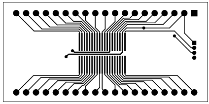
It refers to a picture of how and where copper remains on every layer with black representing copper and the rest being clear. It's not just copper on a PCB because copper tends to get oxidized easily when exposed to air making it difficult to adhere with solder. Generally, there is a solder mask, green in colour over the copper as well as the legend, silkscreen or nomenclature, which is comprised of white letters. Gerber files also provide information regarding holes, cutouts in a stencil, solder mask paint and the silkscreen.
Manufacturers typically receive about 9 files for every basic 2-layer PCB. These files include:
- Top layer image of copper conductor on the PCB
- Bottom layer image of copper tracks on the PCB
- Image of the solder mask for the top layer
- Image of the bottom layer solder mask
- Image for the silkscreen on top layer
- Image for the silkscreen on bottom layer
- Information regarding holes (their locations, properties and descriptions). Mostly NPTH and PTH are two separate files.
- Internal cut-outs and various machining operation (e-g: slots, scoring) which are the outline of a board are included
- A file with information regarding name and purpose of each and every of the above mentioned files, mostly named as README.
Related Articles:
Please briefly describe the information you are seeking in the search bar below.