


 English
TURN-KEY PCB ASSEMBLY: BITTELE ELECTRONICS
PCB MANUFACTURING AND ASSEMBLY
Full Turn-Key PCB Manufacturer
You can quickly get quotes and order PCB fabrication and assembly using our online system. Take advantage of exclusive automatic discounts with our tool. Our BOM pricing tool ensures you receive the lowest price for your order.
START A TURN-KEY PCB ORDER
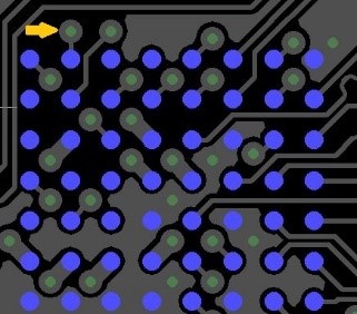
Capabilities for DSBGA and other Complex Components
Bittele offers assembly for a variety of different leadless parts. The chart below outlines some of these parts and our current assembly capabilities. Bittele Electronics is always working to grow our capabilities; if there is a package you do not see below please feel free to contact us.
Our leadless parts assembly capabilities:
| Supported capabilities: | ||
|---|---|---|
| Leadless parts: | BGA (Ball Grid Array) | Pitch >= 0.4mm |
| µBGA (Micro Ball Grid Array) | ||
| CABGA (Chip Array Ball Grid Array) | ||
| CTBGA (Thin Chip Array Ball Grid Array) | ||
| CVBGA (Very Thin Chip Array Ball Grid Array) | ||
| LGA (Land Grid Array) | ||
| VFBGA (Very Fine Pitch Ball Grid Array) | ||
| CSP (Chip scale Package) | ||
| WLCSP (Wafer level chip scale packaging) | ||
| DSBGA (Die-Size Ball Grid Array) | *Under development | |
| Flip Chip | ||
| Passive footprints: | 0201, 0402, 0603, etc. | Size >= 0201 |
| 01005 | *Under development | |
To ensure that the highest level of quality can be maintained for your leadless assembly, Bittele Electronics includes X-Ray inspection for components such as BGA, µBGA, LGA, and CSP. Other testing services such as AOI (Automated Optical Inspection) and Functional testing are also available.
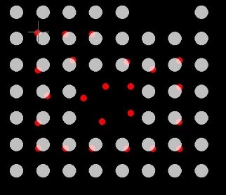
To make efficient use of BGA signal routing in your PCB design, there are two primary methods for routing the traces away from the BGA pad.
1) First is a method known as “Dog Bone fan-out”. This method utilizes short traces to connect the BGA pads to a nearby Via, or, out from underneath the component.
2) For small pitch parts (such as uBGA), there may not be room between the BGA pads to incorporate the previous method in your design. In this case, the second method is known as “Via in Pad fan-out”. This method places the via directly on the pads of the BGA components. Typically, these vias will be filled with a non-conductive epoxy and then plated over with copper. This method does come with some additional cost and leadtime, as the via will need to be filled, however it does help to reduce board size by reducing the complexity of the traces that will need to be routed for the BGA component.
Another option to consider for your project is utilizing a socket for leadless parts. This option is useful for prototyping, as it allows you to remove and replace the IC for programming / testing while your design is finalized. These sockets are available in both surface mount and through hole designs.
Related Articles:
Please briefly describe the information you are seeking in the search bar below.