


 English
TURN-KEY PCB ASSEMBLY: BITTELE ELECTRONICS
PCB MANUFACTURING AND ASSEMBLY
Full Turn-Key PCB Manufacturer
You can quickly get quotes and order PCB fabrication and assembly using our online system. Take advantage of exclusive automatic discounts with our tool. Our BOM pricing tool ensures you receive the lowest price for your order.
START A TURN-KEY PCB ORDER
X-Ray Inspection
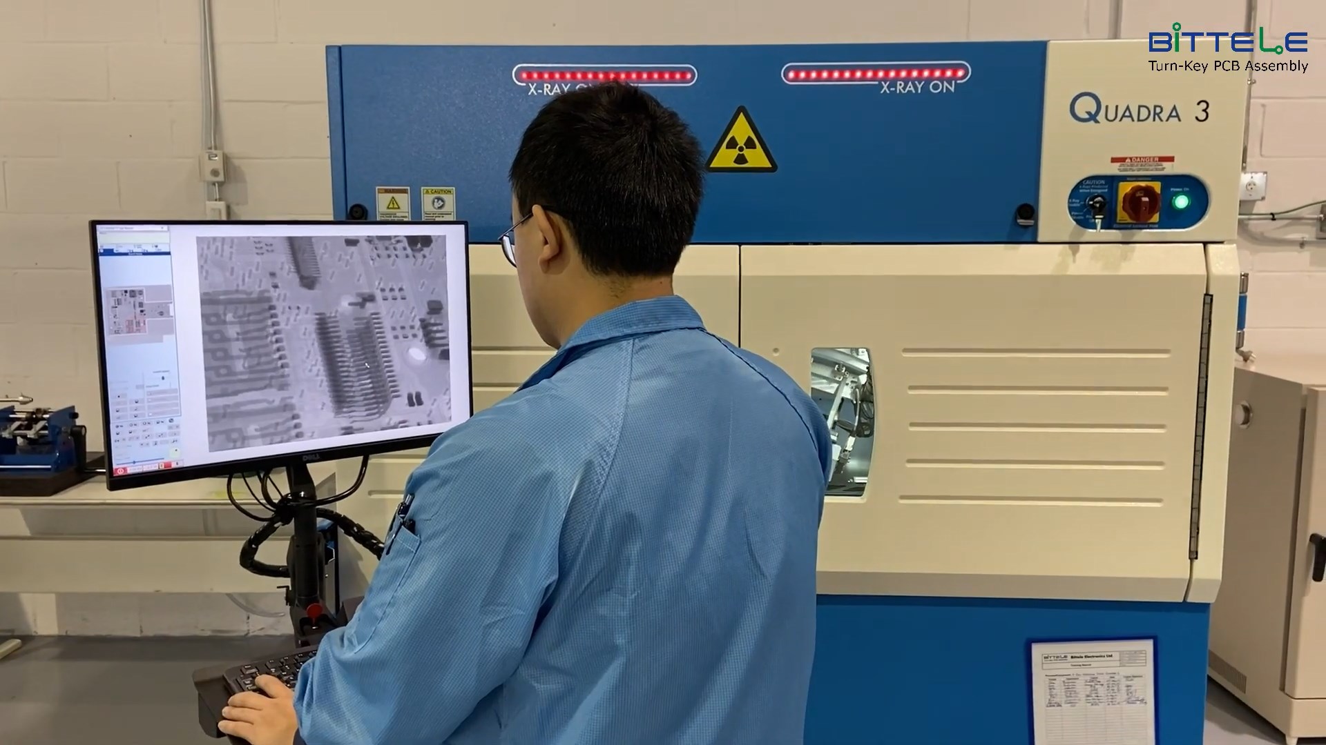
For designs including BGA Assembly, as well as QFN or other lead-less package types, connections to the PCB are formed beneath the body of the components themselves. As such, visual and AOI testing are not sufficient to verify a robust assembly, and Bittele must employ X-Ray inspection in order to meet quality assurance guidelines. Bittele added 3D Automatic X-Ray Inspection (AXI) as a verification technique in early 2016, and this service is now included by default on any Bittele quotations including the assembly of lead-less packages, such as those mentioned above.
Not only does X-Ray inspection detect issues in PCB assembly, but the analysis of an X-Ray image can help to determine the root cause of a given defect, such as insufficient solder paste, skewed part placement, or improper reflow soldering profile. This technique contributes greatly to Bittele’s Quality Management strategy for complex components.
Since X-Ray Inspection is included by default on all quotations requiring lead-less package assembly, clients need only include the lead-less parts on their Bill of Materials when they submit a PCB Assembly project for quoting. To be sure that a particular part will be subjected to this testing, a note can be added to the relevant BOM row, or clients can mention this requirement to their Bittele account manager.
For any further questions regarding X-Ray Inspection, feel free to reach out to sales@7pcb.com.