


 English
TURN-KEY PCB ASSEMBLY: BITTELE ELECTRONICS
PCB MANUFACTURING AND ASSEMBLY
Full Turn-Key PCB Manufacturer
You can quickly get quotes and order PCB fabrication and assembly using our online system. Take advantage of exclusive automatic discounts with our tool. Our BOM pricing tool ensures you receive the lowest price for your order.
START A TURN-KEY PCB ORDER
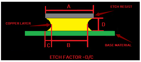
How Etch Factor affects Trace width and spacing
In the PCB manufacturing process, copper has to be removed from solid copper sheets in order to form traces. One of the most common ways the excess copper is removed from the copper sheets is through a process called etching. The copper traces and other features that are to be kept are covered in a resist that protects the copper from the chemical etching solution. As the solution removes the exposed copper some of the copper between the laminate/base material and the resist is also removed, in other words, the ‘walls’ of the copper trace have material etched from them. This is called undercut, when you divide the thickness of the base copper by the amount of undercut you get a value known as the etch factor(D/C in the figure below).
The significance of this is that trace dimensions are specifically chosen so that they behave in a specific way. However if the etch factor is not taken into consideration then the trace is actually thinner than required, leading to a PCB that does not behave as designed.
At Bittele our experienced CAM Engineers increase the size of the traces according to the etch factor so that post etching the traces meet the requirements of your project, this is called etch compensation.
This size increase of the traces is one very important reason why we have requirements for the minimum space that is needed between various copper features.
According to Bittele’s procedures, the etch factor for outer layers is 1.4 and the etch factor for inner layers is 2.5.
Related Articles:
Please briefly describe the information you are seeking in the search bar below.