


 English
TURN-KEY PCB ASSEMBLY: BITTELE ELECTRONICS
PCB MANUFACTURING AND ASSEMBLY
Full Turn-Key PCB Manufacturer
You can quickly get quotes and order PCB fabrication and assembly using our online system. Take advantage of exclusive automatic discounts with our tool. Our BOM pricing tool ensures you receive the lowest price for your order.
START A TURN-KEY PCB ORDER
High Voltage PCB Design Tips
When drawing a PCB layout, it is very important to provide suitable clearance between traces and provide enough space between the components, especially in high voltage applications, in order to avoid any electrical arcing and breakdowns.
Before designing the circuit, the designer should become familiar with the following technical terminology:
- Functional insulation -- the insulation only required for circuit operation. It does not imply safety protection.
- Basic insulation
- Supplementary insulation
- Double insulation
- Reinforced insulation
- Clearance
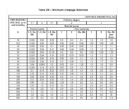
- Creepage distance
- Altitude
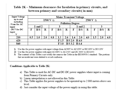
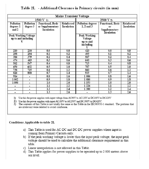
The grade of insulation, PCB type, environment and altitude will affect the clearance and creepage
The PCB designer should follow safety standards such as UL60950-1(USA) or CSA 22.3 (Canada)
Related Articles:
Please briefly describe the information you are seeking in the search bar below.