


 English
TURN-KEY PCB ASSEMBLY: BITTELE ELECTRONICS
PCB MANUFACTURING AND ASSEMBLY
Full Turn-Key PCB Manufacturer
You can quickly get quotes and order PCB fabrication and assembly using our online system. Take advantage of exclusive automatic discounts with our tool. Our BOM pricing tool ensures you receive the lowest price for your order.
START A TURN-KEY PCB ORDER
How to Generate Gerber Files from KiCAD
What is KiCad?
KiCad is a free, easy to download software that is used for electronic design automation (EDA) and computer aided design (CAD). While using this program, PCB design schematics can be realized from their electrical circuits. Within, there are tools that allow the creation of a bill of materials (BOM), artwork, 3D view of the PCB + components and gerber files. This documents purpose will be to guide Bittele’s clients through the step by step process specifically for generating the gerber files using KiCad. Similarly, see our guide for exporting gerbers using another commonly used program (Eagle).
What are Gerber files?
Gerber files are the artwork of the layers that will be used to construct the board once it’s being fabricated. The industry standard file type used for manufacturing and assembling PCB’s are gerber file types. Therefore, they are easily recognized and processed by our manufacturing equipment.
Generating Gerber Files
This guide assumes that you have finished designing your PCB within KiCad and are ready to export the gerber files.
1) Select the ‘Plot’ button (located next to the printer icon).
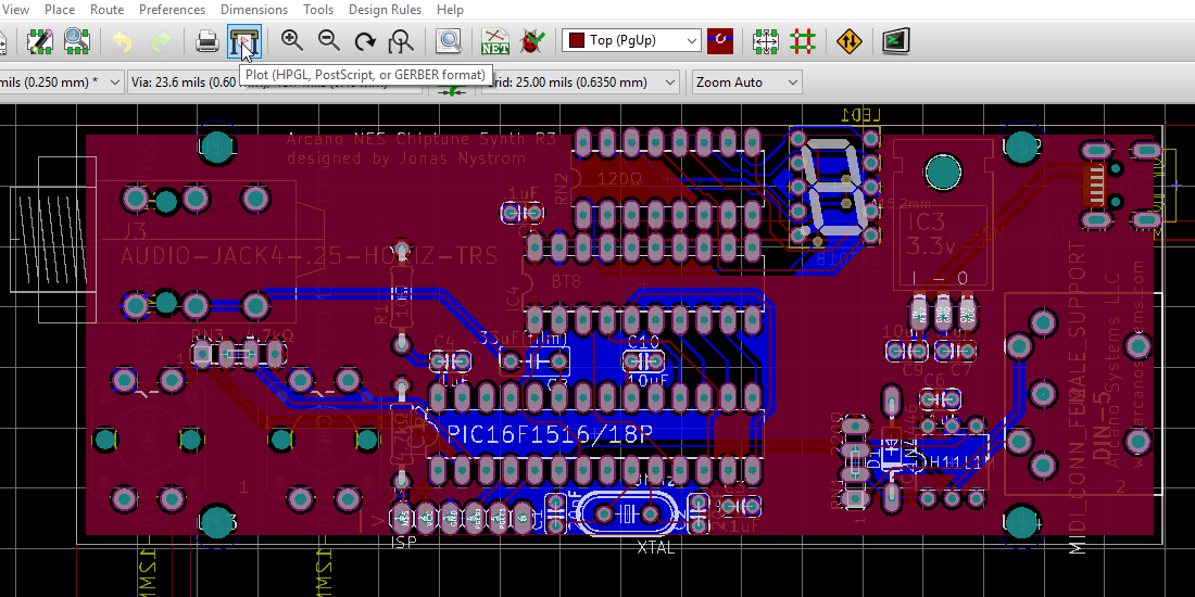
This will open the plot window.
The image above shows the many different layers that are used in this example project. In general, there are only 10 layers that are required for PCB fabrication and assembly (paste layers not required for fabrication only):
- Top Copper (Top) + Top Soldermask (F.Mask) + Top Silkscreen (F.SilkS) + Top Paste (F.Paste)
- Bottom Copper (Bottom) + Bottom Soldermask (B.Mask) + Bottom Silkscreen (B.SilkS) + Bottom Paste (B.Paste)
- Board outline (Edge.Cuts)
- Drill file (not shown in image above)
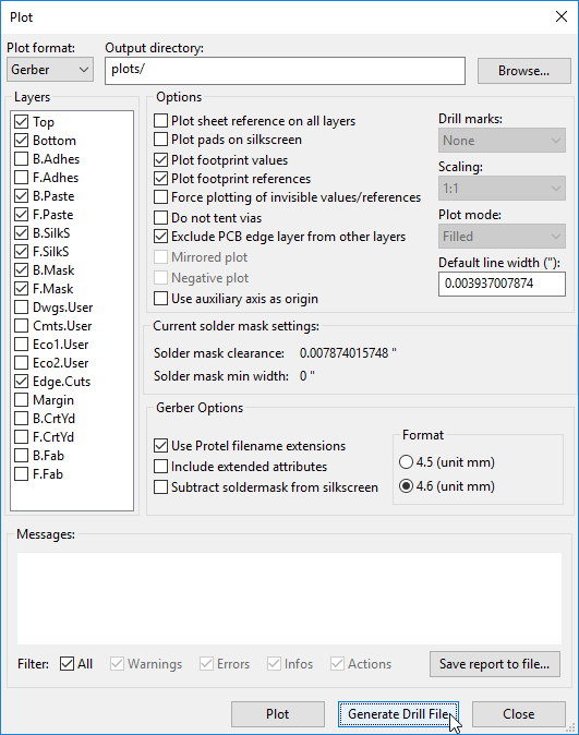
2) Make sure the Plot format is set to ‘Gerber’ and all the aforementioned layers have been selected. Next, you will click on the ‘Generate Drill File’ button. You will be using the default values here. Click on ‘Drill File’ or press enter to generate the drill file (see image below):
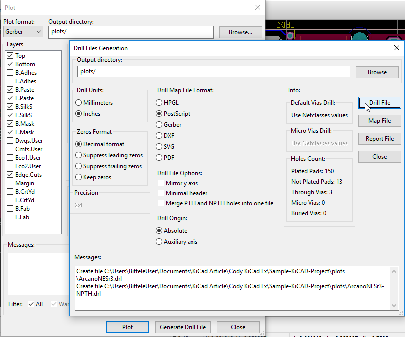
3) Under the messages window will show where the drill files have now been generated. Click on the close button to return to the previous window. Click on ‘Plot’ (beside Generate Drill File). The gerber files for the layers will be generated (shown once again under the messages window), then click ‘Close’.
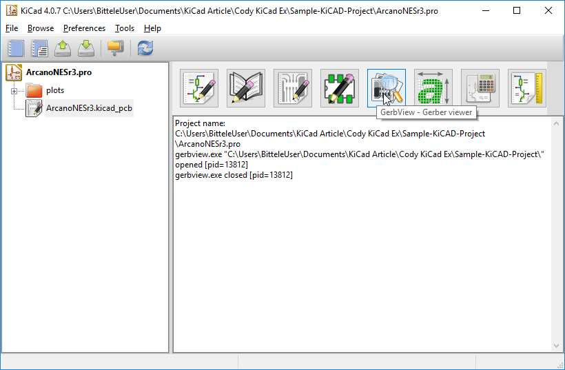
4) Once your gerber files have been generated, they can be reviewed to catch any potential errors before being sent to us for a PCB fabrication quote. Return to the main KiCad project window and click on the GerbView – Gerber viewer button (see image below):
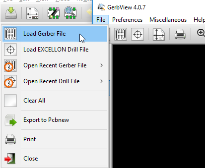
5) On the window that pops up, click ‘File’ > ‘Load Gerber File’.
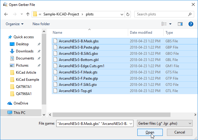
6) Select all of the layers shown and click ‘Open’.
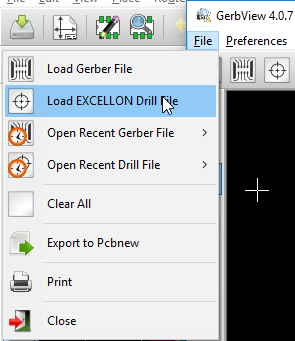
7) In the same manner, click on ‘File’ > ‘Load EXCELLON Drill File’.
8) Select the drill file(s) and click ‘Open’.
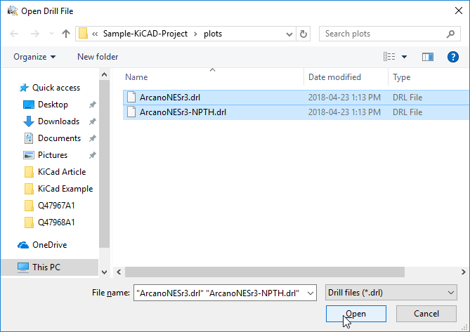
Notice here that 2 drill files have been created. The first represents ‘plated drill holes’ while the second represents the ‘non-plated drill holes’. This will lead us to seeing 11 files instead of 10 files later.
9) Once all of your layers have been imported into GerbView, you can perform all your final checks (you can view each layer one by one and so on). Once you are satisfied that your design is correct, you will be ready to quote and order your boards.
10) Navigate to the directory on your computer where your KiCad project resides. Select and zip the following 11 files:
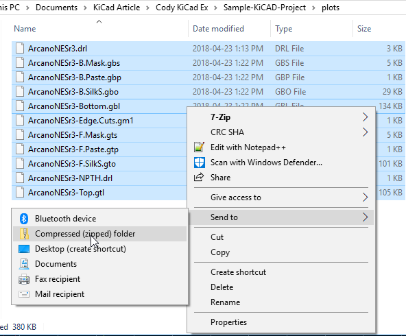
A list explaining each type of file can be seen below:
- *.drl - Drill file
- *.gbs - Gerber Bottom Soldermask
- *.gbp - Gerber Bottom Paste
- *.gbo - Gerber Bottom Silkscreen (Overlay)
- *.gbl - Gerber Bottom Layer
- *.Edge.Cuts.gm1 - Board Outline (Gerber Mechanical 1)
- *.gts - Gerber Top Soldermask
- *.gtp - Gerber Top Paste
- *.gto - Gerber Top Silkscreen (Overlay)
- *.drl - Drill file
- *.gtl - Gerber Top Layer
These are all the production files that we require in order to produce your quote and fabricate your boards. We will then process the quote once the order has been made to have the boards fabricated in our facilities in China.
This guide’s aim has been to describe the procedure for generating Gerber files from KiCad as simply and completely as possible. If you still find yourself unclear on any part of the process, please do not hesitate to contact a member of the Bittele sales team by sending an email to sales@7pcb.com, or calling our Toronto office at 1-416-800-7540. We are happy to help with any of your queries.
Related Articles:
Please briefly describe the information you are seeking in the search bar below.