


 English
TURN-KEY PCB ASSEMBLY: BITTELE ELECTRONICS
PCB MANUFACTURING AND ASSEMBLY
Full Turn-Key PCB Manufacturer
You can quickly get quotes and order PCB fabrication and assembly using our online system. Take advantage of exclusive automatic discounts with our tool. Our BOM pricing tool ensures you receive the lowest price for your order.
START A TURN-KEY PCB ORDER
DFM Analysis on Wave Soldering Quality
I. Characteristics of Modern Wave Soldering in Electronic Assembly
1. Evolution of Wave Soldering in Modern Assembly
Modern electronic assembly has evolved around Surface Mount Technology (SMT), distinguishing it significantly from traditional assembly methods. Consequently, wave soldering today is no longer limited to Through-Hole Technology (THT) or SMT alone, it is now addresses the complexities of mixed SMT and THT assemblies. This shift has made Design for Manufacturability (DFM) increasingly critical. Insufficient DFM can severely compromise wave soldering quality and production efficiency, and in extreme cases, render a product unmanufacturable. Such challenges are especially prevalent in OEM environments where contract manufacturing is common.
2. Importance of Good DFM in PCBA Production
DFM focuses on aligning the relationship between a product’s board design and the manufacturing system. Integrating DFM principles early in the design phase helps reduce development time and costs, improves production yield, and ensures product reliability.
It is widely recognized that up to 80% of manufacturing costs and quality characteristics are locked in during the design phase. Therefore, integrating manufacturability considerations early is essential.
Effective DFM enables manufacturers to reduce defects, simplify processes, shorten production cycles, lower costs, improve quality control, and enhance product reliability and competitiveness.
Successful PCBA designs consistently demonstrate that only by addressing manufacturability, usability, testability, cost-efficiency, and quality stability in the early stage can “zero-defect design” be achieved. Design flaws often lead to systematic quality issues that are difficult to resolve during production, what’s known as “design-born defects.”
II. DFM Guidelines and Considerations for PCB Layout
1. PCB Stress Distribution During Assembly
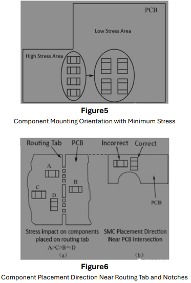
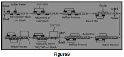
From a structural standpoint, PCBs are inherently fragile. The combine materials with vastly different coefficients of thermal expansion and elastic residue, mounted on a flexible laminate is prone to stress concentration, especially at sharp corners.
During cutting, clamping, connector insertion, and soldering, excessive PCB warpage can introduce mechanical stress at solder joints, leading to component damage such as solder cracks or solder joint fatigue as shown in Figures 1 to 4 below.
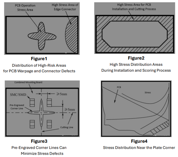
There is currently a standard that determines how much PCB warpage is allowed before components are damaged. However, stress cracking of components during wave soldering (such as ceramic capacitors) is correlates to PCB warpage and varies with different substrate materials. Therefore, control and management of assembly warpage is required during both manufacturing and assembly process.
2. Component Placement Strategy
Proper component placement is crucial for minimizing wave soldering defects. Recommended practices during component placement should be met that’s includes the following
- A) Avoid placing components near high-stress areas, such as PCB corners and edges. Maintain at least 5 mm clearance from the board edge.
- B) Distribute components evenly, especially those with high thermal mass, to prevent thermal gradients.
- C) Place power components near the board edge for better heat dissipation.
- D) Avoid placing expensive or sensitive components near stress-prone areas like connectors, mounting holes, or V-score.
- E) Large PCBs are more prone to warping, and even well-placed components may still be affected. Components aligned perpendicular to the stress gradient are especially vulnerable.
3. Optimal Assembly Structures for Mixed Assemblies
With increasing PCBA density for modern electronic products, the simple SMT or THT assemblies was replaced by mixed SMT/THT assemblies have become standard. Common configurations includes
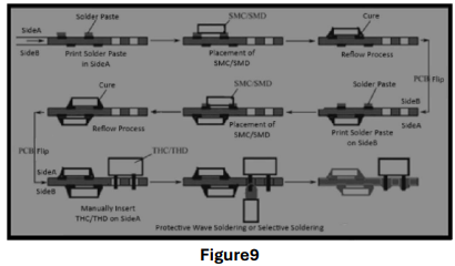
- A) SMT/THT Hybrid: Simplest form, often completed with a single wave soldering process is required. Its typical process flow is shown in the Figure7 below.
- B) (THT, SMT)/SMT: Used when there is special requirement for number of parts quantity or weight, but PCBA geometry is strictly limited. Two standard process flows to be used.
- b.1) Reflow on Side A, Wave Solder on Side B: Place large or sensitive components such as QFP, PLCC and components that are not suitable for wave soldering on Side A while small, sealed components such as chip resistors, SOP with less than 28 pins and pitch of not less than 0.8 mm are completely sealed on Side B.
- b.2) Reflow on Both Sides + Selective or Protective Wave Soldering: Used for complex assemblies requiring additional protection.
4. Power/Ground Traces and Via Design
- A) Power and Ground Traces
Due to different thermal expansion coefficient and thermal conductivity of copper foil and prepreg materials on PCB, unevenly distributed copper foil layers can easily cause large delamination and warping of PCB under preheating and soldering temperature. The following requirements should be met during design: - a.1) Large power and ground areas should use cross-hatching design to reduce thermal stress.
- a.2) Copper distribution should be balanced across layers to minimize warping.
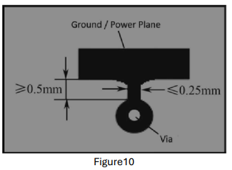
- B) Vias
The main function of vias is to achieve electrical interconnection between PCB layers. As the SMT density has been greatly improved and PCBs are constantly developing towards multi layers board, the role of vias is becoming more and more important and the quantity is increasing. The layout and requirements of vias in the design are as follows - b.1) Maintain at least 0.63 mm clearance between vias and pads to prevent solder wicking.
- b.2) Avoid placing vias under SMC/SMD components to prevent solder voids or solder entrapment.
- b.3) When connecting vias to power/ground, use necked traces (≤0.25 mm wide, ≥0.5 mm long) to control heat flow as shown in Figure10.
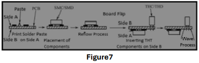
5. Design Considerations When Using Panelization
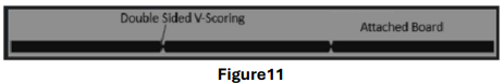
When using panelization, the components near the edge of the board will inevitably produce a large stress, thereby causing the solder joints and components to separate or having cracked. Since SMC/SMD does not have a flexible solder to eliminate the mechanical stress generated by the PCB, it is more likely to cause damage to SMC/SMD. Therefore, the use of a panelized board can minimize the warping deformation during de-paneling and eliminate the stress and defects of the components. De-paneling can be done by using double-sided V-scoring. The depth of the V-score (the sum of the score depths on both sides) is about 1/3 of the board thickness. The score size must be accurate, and the depth must be uniform to minimize warpage and stress during de-paneling, as shown in the Figure11below.
Note:
This article is the first in a series. Future sections will explore DFM considerations related to test pad design, component spacing, solder mask layout, and more.
To make an inquiry, please send your PCB Design Files and any special requirements to sales@7pcb.com.
Related Articles:
Please briefly describe the information you are seeking in the search bar below.