


 English
TURN-KEY PCB ASSEMBLY: BITTELE ELECTRONICS
PCB MANUFACTURING AND ASSEMBLY
Full Turn-Key PCB Manufacturer
You can quickly get quotes and order PCB fabrication and assembly using our online system. Take advantage of exclusive automatic discounts with our tool. Our BOM pricing tool ensures you receive the lowest price for your order.
START A TURN-KEY PCB ORDER
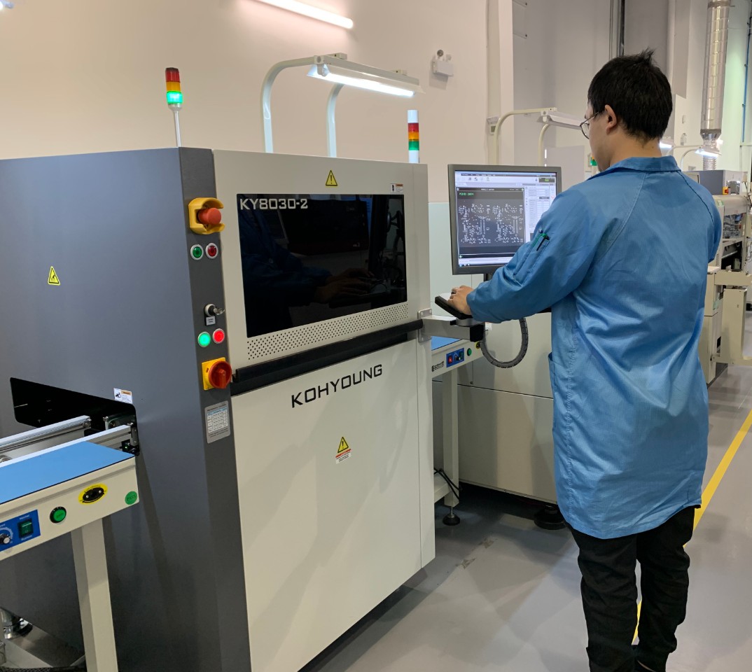
3D Solder Paste Inspection in the PCB Assembly Process
We conduct 3D solder paste inspections (SPI) for every SMT circuit board assembled in Bittele Electronics. Alongside our first article inspection (FAI,) automated optical inspection (AOI,) 3D AOI, X-ray inspection and functional testing procedures, 3D SPI ensures that every PCB we assemble is guaranteed to be free of any solder joint defects.
After going through our solder paste printer, each PCB is not only visually inspected, but passed through our automated 3D SPI machine. The system features a communication interface to the solder paste printer and is programmed by our qualified assembly technicians, using customer-provided Gerber and CAD files. Every board is examined with a computer-controlled camera, in greater detail than possible with the naked eye. Each SMT pad is analyzed for the correct volume, height and, with respect to the CAD design’s layout, the position and location of solder paste.
If the circuit board fails 3D SPI, the machine will generate a failure report and feed it directly to the solder paste printer through its communication interface. This report contains programming code to automatically adjust the print offset, paste volume and other parameters to correct any failures in the solder printing process. Once the PCB passes inspection, it can then proceed to the pick-and-place process.
Even though our first article inspection process is meant to ensure our solder printers and assembly equipment are properly calibrated, our 3D SPI process exists to ensure continuous, consistent, quality results for every PCB we process in our solder printers, while eliminating the possibility of SMT soldering defects after the pick-and-place, AOI and solder reflow processes. In our pursuit to perfect our assembly procedures for both speed and quality, our customers can rest assured that we will never leave anything to chance.