


 English
TURN-KEY PCB ASSEMBLY: BITTELE ELECTRONICS
PCB MANUFACTURING AND ASSEMBLY
Full Turn-Key PCB Manufacturer
You can quickly get quotes and order PCB fabrication and assembly using our online system. Take advantage of exclusive automatic discounts with our tool. Our BOM pricing tool ensures you receive the lowest price for your order.
START A TURN-KEY PCB ORDER
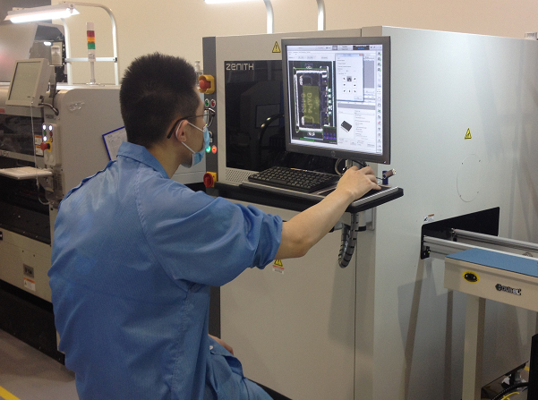
3D Automated Optical Inspection in the PCB Assembly Process
As part of our comprehensive quality management toolkit, Bittele uses 3D automated optical inspection (AOI) to ensure that every SMT circuit board we assemble is done right the first time. Regardless of design complexity, 3D AOI is one of the many ways that we maintain strict levels of PCB assembly quality, in addition to FAI, 3D solder paste inspection (SPI,) functional testing and X-ray inspection.
3D AOI is a method of inspecting SMT circuit boards at the component level, before soldering, with the help of a camera and computer to map each board in 3D. The system is programmed by our trained assembly technicians, using customer-provided Gerber files, CAD files and our own digital library of component specifications. All of this allows the 3D AOI system to compare the component layout between the assembled PCB and original CAD design.
The major benefit of 3D AOI is that it mitigates errors in the pick-and-place process during PCB assembly. If a component was placed in the wrong orientation or location of the board, or if any component is slightly skewed out of place, the 3D AOI system will pick up this issue and prompt our assembly technicians of this error, which must be rectified on both the board and in the pick-and-place machine’s programming. This goes together with our first article inspection process, ensuring that we perfect the entire production run.
Another benefit is that physical dimensional tolerances are ensured to within a few mils, thanks to the automated process of comparing each component’s height and placement to our library of parts specifications. This ensures that our customers can properly take advantage of their PCB design’s form factor, when putting their circuit boards into practical use. Whether each board is to be installed into a custom-engineered enclosure, or just about anywhere else, 3D AOI will guarantee that all boards we produce will meet your dimensional tolerancing needs.